


DS33R11 Ethernet Mapper with Integrated T1/E1/J1 Transceiver
251 of 344
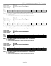
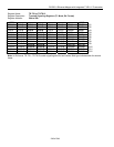
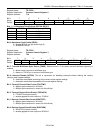
Register Name:
TR.CCR1
Register Description:
Common Control Register 1
Register Address:
70h
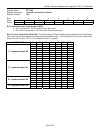
Bit # 7 6 5 4 3 2 1 0
Name MCLKS CRC4R SIE ODM DICAI TCSS1 TCSS0 RLOSF
Default 0 0 0 0 0 0 0 0
Bit 7: MCLK Source (MCLKS). Selects the source of MCLK
0 = MCLK is source from the MCLK pin
1 = MCLK is source from the TSYSCLK pin
Bit 6: CRC-4 Recalculate (CRC4R)
0 = transmit CRC-4 generation and insertion operates in normal mode
1 = transmit CRC-4 generation operates according to G.706 intermediate path recalculation method
Bit 5: Signaling Integration Enable (SIE)
0 = signaling changes of state reported on any change in selected channels
1 = signaling must be stable for three multiframes in order for a change of state to be reported
Bit 4: Output Data Mode (ODM)
0 = pulses at TPOSO and TNEGO are one full TCLKO period wide
1 = pulses at TPOSO and TNEGO are one-half TCLKO period wide
Bit 3: Disable Idle Code Auto Increment (DICAI). Selects/deselects the auto-increment feature for the transmit
and receive idle code array address register. See Section
10.10.
0 = addresses in TR.IAAR register automatically increment on every read/write operation to the TR.PCICR
register
1 = addresses in TR.IAAR register do not automatically increment
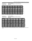
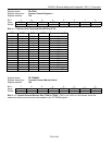
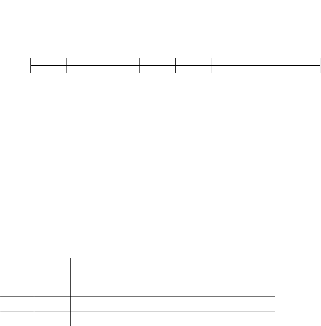
Bit 2: Transmit Clock Source Select Bit 0 (TCSS1)
TCSS1 TCSS0 Transmit Clock Source
0 0 The TCLKT pin is always the source of transmit clock.
0 1
Switch to the clock present at RCLKO when the signal at the TCLKT pin
fails to transition after 1 channel time.
1 0
Use the scaled signal present at MCLK as the transmit clock. The
TCLKT pin is ignored.
1 1
Use the signal present at RCLKO as the transmit clock. The TCLKT pin
is ignored.
Bit 1: Transmit Clock Source Select Bit 0 (TCSS0)
Bit 0: Function of the RLOS/LOTC Output (RLOSF)
0 = receive loss of sync (RLOS)
1 = loss-of-transmit clock (LOTC)