DS33R11 Ethernet Mapper with Integrated T1/E1/J1 Transceiver
136 of 344
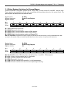
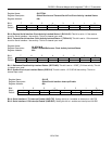
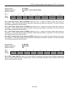
Register Name:
GL.RTCAL
Register Description:
Global Receive and Transmit Serial Port Clock Activity Latched Status
Register Address:
04h
Bit # 7 6 5 4 3 2 1 0
Name - - - RLCALS1 - - - TLCALS1
Default - - - - - - - -
Bit 4: Receive Serial Interface Clock Activity Latched Status 1 (RLCALS1) This bit is set to 1 if the receive
clock for Serial Interface 1 has activity. This bit is cleared upon read.
Bit 0: Transmit Serial Interface Clock Activity Latched Status 1 (TSCALS1) This bit is set to 1 if the transmit
clock for Serial Interface 1 has activity. This bit is cleared upon read.
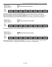
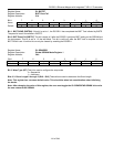
Register Name:
GL.SRCALS
Register Description:
Global SDRAM Reference Clock Activity Latched Status
Register Address:
05h
Bit # 7 6 5 4 3 2 1 0
Name - - - - - - REFCLKS SYSCLS
Default - - - - - - - -
Bit 1: Reference Clock Activity Latched Status (REFCLKS) This bit is set to 1 if REF_CLK has activity. This bit
is cleared upon read.
Bit 0: System Clock Input Latched Status (SYSCLS) This bit is set to 1 if SYSCLKI has activity. This bit is
cleared upon read.
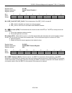
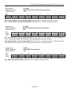
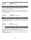
Register Name:
GL.LIE
Register Description:
Global Serial Interface Interrupt Enable
Register Address:
06h
Bit # 7 6 5 4 3 2 1 0
Name - - - LIN1TIE - - - LIN1RIE
Default 0 0 0 0 0 0 0 0
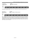
Bit 4: Serial Interface 1 TX Interrupt Enable (LINE1TIE) Setting this bit to 1 enables an interrupt on LIN1TIS
Bit 0: Serial Interface 1 RX Interrupt Enable (LINE1RIE) Setting this bit to 1 enables an interrupt on LIN1RIS


