DS33R11 Ethernet Mapper with Integrated T1/E1/J1 Transceiver
142 of 344
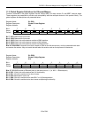
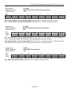
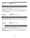
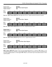
Register Name:
GL.SDMODE2
Register Description:
Global SDRAM Mode Register 2
Register Address:
3Bh
Bit # 7 6 5 4 3 2 1 0
Name - - - - - LTMOD2 LTMOD1 LTMOD0
Default 0 0 0 0 0 0 1 0
Bits 0 - 2: CAS Latency Mode (LTMOD0 - LTMOD2) These bits are used to setup CAS Latency
Note: Only CAS Latency of 2 or 3 is allowed
Note: This register has a nonzero default value. This should be taken into consideration when initializing
the device.
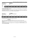
Note: After changing the value of this register, the user must toggle the GL.SDMODEWS.SDMW bit to write
the new values to the SDRAM.
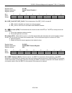
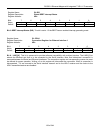
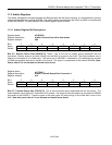
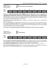
Register Name:
GL.SDMODEWS
Register Description:
Global SDRAM Mode Register Write Status
Register Address:
3Ch
Bit # 7 6 5 4 3 2 1 0
Name - - - - - - - SDMW
Default 0 0 0 0 0 0 0 0
Bit 0: SDRAM Mode Write (SDMW) Setting this bit to 1 will write the current values of the mode control and
refresh time control registers to the SDRAM. The user must clear this bit and set it again for subsequent write
operations.
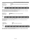
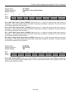
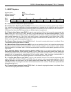
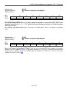
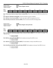
Register Name:
GL.SDRFTC
Register Description
Global SDRAM Refresh Time Control
Register Address:
3Dh
Bit # 7 6 5 4 3 2 1 0
Name SREFT7 SREFT6 SREFT5 SREFT4 SREFT3 SREFT2 SREFT1 SREFT0
Default 0 1 0 0 0 1 1 0
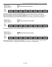
Bits 0 - 7: SDRAM Refresh Time Control (SREFT0 – SREFT7) These 8 bits are used to control the SDRAM
refresh frequency. The refresh rate will be equal to this register value x 8 x 100MHz.
Note: This register has a nonzero default value. This should be taken into consideration when initializing
the device.
Note: After changing the value of this register, the user must toggle the GL.SDMODEWS.SDMW bit to write
the new values to the SDRAM.


