DS33R11 Ethernet Mapper with Integrated T1/E1/J1 Transceiver
46 of 344
9.2 Resets and Low Power Modes
The external RST pin and the global reset bit in GL.CR1 create an internal global reset signal. The global reset
signal resets the status and control registers on the chip (except the
GL.CR1.RST bit) to their default values and
resets all the other flops to their reset values. The processor bus output signals are also placed in high-impedance
mode when the RST pin is active (low). The global reset bit (
GL.CR1.RST) stays set after a one is written to it, but
is reset to zero when the external RST pin is active or when a zero is written to it. Allow 5ms after initiating a reset
condition for the reset operation to complete.
The Serial Interface reset bit in LI.RSTPD resets all the status and control registers on the serial interface to their
default values, except for the
LI.RSTPD.RST bit. The serial interface includes the HDLC encoder/decoder, X86
encoder and decoder and the corresponding serial port. The serial interface reset bit (
LI.RSTPD.RST) stays set
after a one is written to it, but is reset to zero when the global reset signal is active or when a zero is written to it.
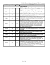
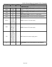
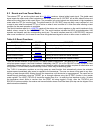
Table 9-2. Reset Functions
RESET FUNCTION LOCATION COMMENTS
Hardware Device Reset
RST Pin
Transition from a logic 0 to a logic 1 resets the device.
Hardware JTAG Reset
JTRST Pin
Resets the JTAG test port.
Global Software Reset GL.CR1 Writing to this bit resets the device.
Serial Interface Reset LI.RSTPD Writing to this bit resets the Serial Interface.
Queue Pointer Reset GL.C1QPR Writing to this bit resets the Queue Pointers.
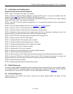
There are several features in the DS33R11 to reduce power consumption. The reset bit in the LI.RSTPD register
minimizes power usage in the Serial Interface. Additionally, the RST pin or
GL.CR1.RST bit may be held in reset
indefinitely to keep the device in a low-power mode. Note that exiting a reset condition requires re-initialization and
configuration. For the lowest possible standby current, clocks may be externally gated.
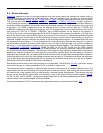
The T1/E1/J1 transceiver contains an on-chip power-up reset function that automatically clears the writeable
register space immediately after power is supplied to the transceiver. The user can issue a chip reset at any time.
Issuing a reset disrupts traffic flowing through the transceiver until the device is reprogrammed. The reset can be
issued through hardware using the TSTRST pin or through software using the SFTRST function in the master
mode register. The LIRST (TR.LIC2.6) should be toggled from 0 to 1 to reset the line interface circuitry. (It takes
the transceiver about 40ms to recover from the LIRST bit being toggled.) Finally, after the TSYSCLK and
RSYSCLK inputs are stable, the receive and transmit elastic stores should be reset (this step can be skipped if the
elastic stores are disabled).


