


DS33R11 Ethernet Mapper with Integrated T1/E1/J1 Transceiver
335 of 344
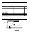
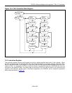
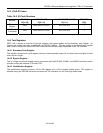
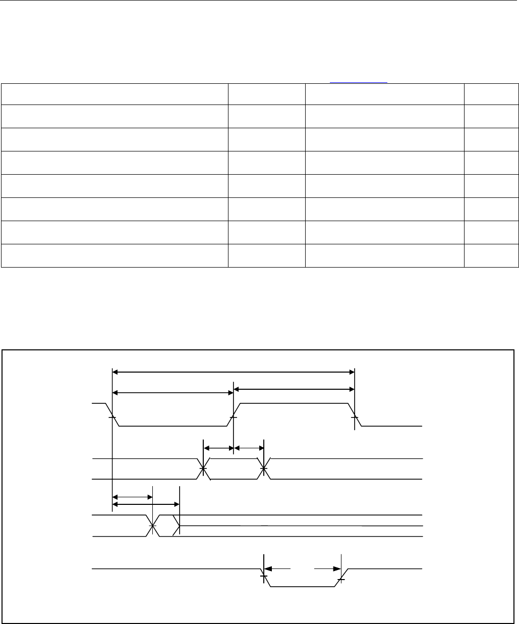
13.12 JTAG Interface Timing
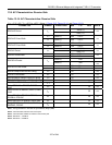
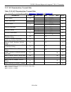
Table 13-17. JTAG Interface Timing
(VDD3.3 = 3.3V ±5%,VDD1.8 = 1.8V ±5%, T
j
= -40°C to +85°C.) (Note 1, Figure 13-20)
PARAMETER SYMBOL MIN TYP MAX UNITS
JTCLK Clock Period t1 1000 ns
JTCLK Clock High:Low Time (Note 2) t2 : t3 50 500 ns
JTCLK to JTDI, JTMS Setup Time t4 2 ns
JTCLK to JTDI, JTMS Hold Time t5 2 ns
JTCLK to JTDO Delay t6 2 50 ns
JTCLK to JTDO HIZ Delay t7 2 50 ns
t8 100 ns
JTRST Width Low Time
Note 1: Timing parameters in this table are guaranteed by design (GBD).
Note 2: Clock can be stopped high or low
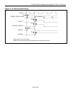
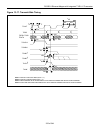
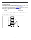
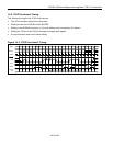
Figure 13-20. JTAG Interface Timing Diagram
JTCLK
t1
JTD0
t4 t5
t2
t3
t7
JTDI, JTMS
t6
JTRST
t8