DS33R11 Ethernet Mapper with Integrated T1/E1/J1 Transceiver
30 of 344
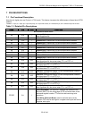
NAME PIN TYPE FUNCTION
SDATA[0] W2
SDATA[1] Y4
SDATA[2] Y2
SDATA[3] Y5
SDATA[4] Y3
SDATA[5] W5
SDATA[6] V5
SDATA[7] W6
SDATA[8] V6
SDATA[9] W4
SDATA[10] V4
SDATA[11] V2
SDATA[12] V3
SDATA[13] V1
SDATA[14] W3
SDATA[15] W1
SDATA[16] Y16
SDATA[17] Y17
SDATA[18] V18
SDATA[19] Y19
SDATA[20] V19
SDATA[21] Y20
SDATA[22] U19
SDATA[23] W20
SDATA[24] U20
SDATA[25] T19
SDATA[26] T20
SDATA[27] Y18
SDATA[28] W19
SDATA[29] V17
SDATA[30] W17
SDATA[31] W16
O
SDRAM Data Bus Bits 0 to 31: The 32 pins of the SDRAM data
bus are inputs for read operations and outputs for write operations.
At all other times, these pins are high-impedance.
Note: All SDRAM operations are controlled entirely by the
DS33R11. No user programming for SDRAM buffering is required.
SDA[0] W14
SDA[1] W12
SDA[2] Y15
SDA[3] W15
SDA[4] Y14
SDA[5] V13
SDA[6] W13
SDA[7] Y12
SDA[8] V12
SDA[9] Y10
SDA[10] V14
SDA[11] W11
O
SDRAM Address Bus 0 to 11: The 12 pins of the SDRAM address
bus output the row address first, followed by the column address.
The row address is determined by SDA0 to SDA11 at the rising
edge of clock. Column address is determined by SDA0-SDA9 and
SDA11 at the rising edge of the clock. SDA10 is used as an auto-
precharge signal.
Note: All SDRAM operations are controlled entirely by the
DS33R11. No user programming for SDRAM buffering is required.
SDMASK[0] Y6
SDMASK[1] V7
SDMASK[2] V16
SDMASK[3] V15
O
SDRAM Mask 0 through 3: When high, a write is done for that
byte. The least significant byte is SDATA7 to SDATA0. The most
significant byte is SDATA31 to SDATA24.
SDCLKO Y8
O
(4mA)
SDRAM CLK Out: System clock output to the SDRAM. This clock
is a buffered version of SYSCLKI.


