DS33R11 Ethernet Mapper with Integrated T1/E1/J1 Transceiver
34 of 344
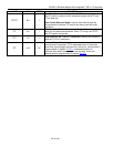
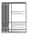
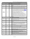
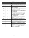
NAME PIN TYPE FUNCTION
ETHERNET MAPPER RECEIVE SERIAL INTERFACE
RSERI H1 I
Receive Serial Data Input to Ethernet Mapper: Receive Serial
data arrives on the rising edge of RCLKI. Normally connected to
RSERO.
RCLKI F2 I
Serial Interface Receive Clock Input to the Ethernet Mapper:
Reference clock for receive serial data on RSERI. Gapped clocking
is supported, up to the maximum RCLKI frequency of 52 MHz.
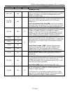
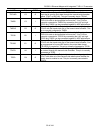
RDEN/
RBSYNC
P2 I
Receive Data Enable for the Ethernet Mapper: The receive data
enable is programmable to block the receive data. The RDEN must
be coincident with the RSERI data bit to be blocked or enabled.
The active polarity of RDEN is programmable in register
LI.RSLCR.
It is recommended for both T1/E1 and T3/E3 applications that use
gapped clocks. The RDEN signal is provided for interfacing to
framers that do not have a gapped clock facility.
Receive Byte Synchronization Input: Provides byte
synchronization input to X.86 decoder. This signal will go high at
the last bit of the byte as it arrives. This signal can occur at
maximum rate every 8 bits. Note that a long as the R11 receives
one RBSYNC indicator. The X.86 receiver will determine the byte
boundary. Hence the R11 does not require a continuous 8 bit sync
indicator. A new sync pulse is required if the byte boundary
changes.
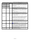
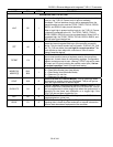
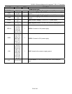
T1/E1/J1 FRAMER/LIU INTERIM SIGNALS
RDCLKI M4 I
Receive Clock Input to the T1/E1/J1 Framer: Clock used to clock
data through the receive-side framer. This pin is normally
connected to RDCLKO. Can be internally connected to RDCLKO
by connecting the LIUC pin high.
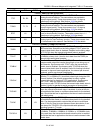
RDCLKO M3 O
Receive Clock Output from the T1/E1/J1 LIU: Buffered
recovered clock from the network. This pin is normally connected to
RDCLKI.
RNEGI L4 I
Receive Negative-Data Input: Sampled on the falling edge of
RDCLKI for data to be clocked through the receive-side framer.
RPOSI and RNEGI can be connected together for an NRZ
interface. Can be internally connected to RNEGO by connecting
the LIUC pin high.
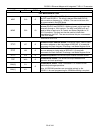
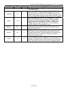
RNEGO N2 O
Receive Negative Data Output from the T1/E1/J1 LIU: Updated
on the rising edge of RDCLKO with the bipolar data out of the line
interface. This pin is normally tied to RNEGI.
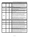
RPOSI J3 I
Receive Positive-Data Input to the T1/E1/J1 Framer: Sampled
on the falling edge of RDCLKI for data to be clocked through the
receive-side framer. RPOSI and RNEGI can be connected together
for an NRZ interface. Can be internally connected to RPOSO by
connecting the LIUC pin high.
RPOSO N3 O
Receive Positive-Data Output from the T1/E1/J1 LIU: Updated
on the rising edge of RDCLKO with bipolar data out of the line
interface. This pin is normally connected to RPOSI.
RDATA H3 O
Receive Data from the T1/E1/J1 Framer: Updated on the rising
edge of RCLKO with the data out of the receive-side framer, before
passing through the Elastic Store.
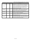
TDCLKI D1 I
Serial Interface Transmit Clock Input for the T1/E1/J1 LIU: Line
interface transmit clock. This pin is normally tied to TCLKO. Can be
internally connected to TCLKO by connecting the LIUC pin high.


