


Rev. 1.00, 05/04, page 95 of 544
Section 7 I/O Ports
This LSI has fifteen I/O ports (ports 1 to 6, 8, 9, and A to G), and one input-only port (port 7).
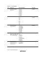
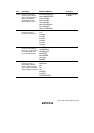
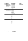
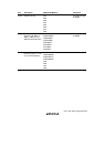
Table 7.1 is a summary of the port functions. The pins of each port also have other functions.
Each port includes a data direction register (DDR) that controls input/output (not provided for the
input-only port) and data registers (DR, ODR) that store output data.
Ports 1 to 3, 6, and A to F have on-chip input pull-up MOSs. For ports A to F, the on/off state of
the input pull-up MOS is controlled by DDR and ODR. Ports 1 to 3 and 6 have DDR and an input
pull-up MOS control register (PCR) to control the on/off state of the input pull-up MOS.
Ports 1 to 6, 8, 9, and A to F can drive a single TTL load and 30-pF capacitive load. All the I/O
ports can drive a Darlington transistor when in output mode. Ports 1, 2, and 3 can drive an LED
(10 mA sink current).
VccB, which is independent of the V
CC
power supply, is supplied to Port A input/output. When the
VccB voltage is 5 V, the pins on port A will be 5-V tolerant.
PA4 to PA7 of port A have bus-buffer drive capability.
P52 in port 5, P97 in port 9, P86 in port 8, P42 in port 4, and PG0 to PG 7 in port G are NMOS
push-pull outputs. P52, P97, P86, P42, and PG0 to PG 7 are thus 5-V tolerant with DC
characteristics dependent on the V
CC
voltage.
For the P42, P52/ExSCK1, P86/SCK1, P97 outputs, and PG0 to PG7, connect pull-up resistors to
pins to raise output-high-level voltage.