


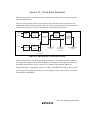

Rev. 1.00, 05/04, page 458 of 544
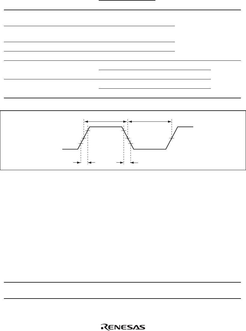
Table 19.3 External Clock Input Conditions
V
CC
=3.0 to 3.6 V
Item Symbol Min Max Unit Test Conditions
External clock input pulse
width low level
t
EXL
40 — ns
External clock input pulse
width high level
t
EXH
40 — ns
External clock rising time t
EXr
— 10 ns
External clock falling time t
EXf
— 10 ns
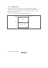
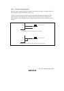
Figure 19.5
0.4 0.6 t
cyc
φ ≥ 5 MHz Clock pulse width low level t
CL
80 — ns φ < 5 MHz
0.4 0.6 t
cyc
φ ≥ 5 MHz Clock pulse width high
level
t
CH
80 — ns φ < 5 MHz
Figure 22.5
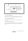
t
EXH
t
EXL
t
EXr
t
EXf
V
CC
× 0.5
EXTAL
Figure 19.5 External Clock Input Timing
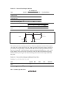
The oscillator and duty correction circuit have a function to adjust the waveform of the external
clock input that is input to the EXTAL pin. When a specified clock signal is input to the EXTAL
pin, internal clock signal output is determined after the external clock output stabilization delay
time (t
DEXT
) has passed. As the clock signal output is not determined during the t
DEXT
cycle, a reset
signal should be set to low to hold it in reset state. Table 19.4 shows the external clock output
stabilization delay time. Figure 19.6 shows the timing of the external clock output stabilization
delay time.
Table 19.4 External Clock Output Stabilization Delay Time
Condition: V
CC
= 3.0 V to 3.6 V, V
SS
= 0 V
Item Symbol Min. Max. Unit Remarks
External clock output stabilization delay
time
t
DEXT
* 500 — µs Figure 19.6
Note: * t
DEXT
includes a RES pulse width (t
RESW
).