


Rev. 1.00, 05/04, page 368 of 544
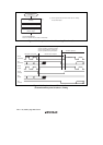
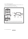
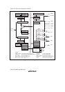
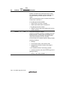
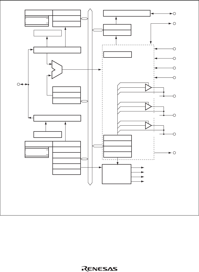
Figure 15.1 shows a block diagram of the LPC.
TWR1–15
IDR3
IDR2
IDR1
H'0060/64
H'0062/66
LADR3
SIRQCR0
SIRQCR1
TWR0MW
TWR1–15
ODR3
ODR2
ODR1
STR3
STR2
STR1
HICR0
HICR1
HICR2
HICR3
TWR0SW
LSCIE
LSCIB
LSCI input
PB1 I/O
LSMIE
LSMIB
LSMI input
PB0 I/O
PMEE
PMEB
PME input
P80 I/O
LAD0 to
LAD3
SERIRQ
CLKRUN
LSCI
LSMI
PME
GA20
LPCPD
LFRAME
LRESET
LCLK
IBFI1
IBFI2
IBFI3
ERRI
Module data bus
Cycle detection
Serial → parallel conversion
Serial ← parallel conversion
Address match
SYNC output
Parallel → serial conversion
Control logic
Internal interrupt
control
HISEL
[Legend]
HICR0 to HICR3: Host interface control registers 0 to 3
LADR3H, 3L: LPC channel 3 address register 3H and 3L
IDR1 to IDR3: Input data registers 1 to 3
ODR1 to DOR3: Output data registers 1 to 3
STR1 to STR3: Status registers 1 to 3
TWR0MW: Two-way register 0MW
TWR0SW: Two-way register 0SW
TWR1 to TWR15: Two-way data registers 1 to 15
SERIRQ0, 1: SERIEQ control registers 0 and 1
HISEL: Host interface select register
Figure 15.1 Block Diagram of LPC