


Rev. 1.00, 05/04, page 138 of 544
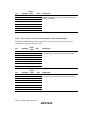
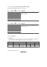
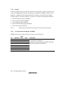
7.13.3 Port E and Port F Input Data Registers (PEPIN, PFPIN)
Reading PEPIN and PFPIN always returns the pin states.
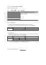
Bit Bit Name
Initial
Value R/W Description
7 PE7PIN Undefined* R
6 PE6PIN Undefined* R
5 PE5PIN Undefined* R
4 PE4PIN Undefined* R
3 PE3PIN Undefined* R
2 PE2PIN Undefined* R
1 PE1PIN Undefined* R
0 PE0PIN Undefined* R
PEPIN indicates the port E state. PEPIN has the same
address as PEDDR. If a write is performed, the port E
settings will change.
Note: * The initial value is determined according to the PE7 to PE0 pin states.
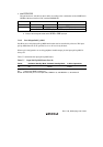
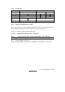
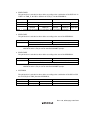
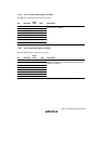
Bit Bit Name
Initial
Value R/W Description
7 PF7PIN Undefined* R
6 PF6PIN Undefined* R
5 PF5PIN Undefined* R
4 PF4PIN Undefined* R
3 PF3PIN Undefined* R
2 PF2PIN Undefined* R
1 PF1PIN Undefined* R
0 PF0PIN Undefined* R
PFPIN indicates the port F state. PFPIN has the same
address as PFDDR. If a write is performed, the port F
settings will change.
Note: * The initial value is determined according to the PF7 to PF0 pin states.
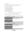
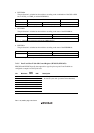
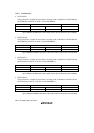
7.13.4 Pin Functions
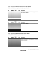
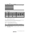
• PF7/TMOY
The pin function is switched as shown below according to the combination of the IOSY bit* in
TCRXY of TMT_Y, the OS3 to OS0 bits in TCSR_Y, and the PF7DDR bit.
IOSY* 0 1
OS3 to OS0 — All 0 Not all 0
PF7DDR 0 1 0 1 —
Pin Function PF7
input pin
PF7
output pin
PF7
input pin
PF7
output pin
TMOY
output pin*
Notes: * The program development tool (emulator) does not support this function.