


Rev. 1.00, 05/04, page 109 of 544
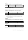
• P43/TMCI1
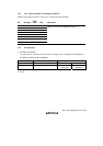
The pin function is switched as shown below according to the state of the P43DDR bit.
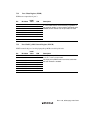
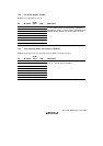
P43DDR 0 1
P43 input pin P43 output pin Pin Function
TMCI1 input pin*
Note: * When the external clock is selected by the bits CKS2 to CKS0 in TCR1 of TMR_1, this
pin is used as the TMCI1 input pin.
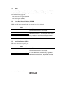
• P42/TMRI0/SDA1
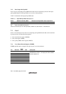
The pin function is switched as shown below according to the combination of the ICE bit in
ICCR of IIC_1, the IIC1AS and the IIC1BS bits in PGCTL*
2
, and the P42DDR bit.
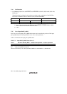
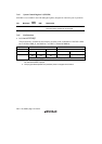
P42ICE = ICE
• (IIC1AS+IIC1BS)*
2
P42ICE*
2
0 1
P42DDR 0 1 —
P42 input pin P42 output pin SDA1 I/O pin Pin Function
TMRI0 input pin*
1
Note: 1. SDA1 is an NMOS-only output, and has direct bus drive capability.
When bits CCLR1 and CCLR0 in TCR0 of TMR_0 are set to 1, this pin is used as the
TMRI0 input pin. When the P42 output pin is set, the output type is NMOS push-pull
output.
2. The program development tool (emulator) does not support the function of PGCTL.
Thus P42ICE is treated as ICE.
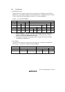
• P41/TMO0
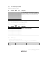
The pin function is switched as shown below according to the combination of the OS3 to OS0
bits in TCSR of TMR_0 and the P41DDR bit.
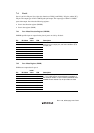
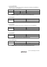
OS3 to OS0 All 0 Not all 0
P41DDR 0 1 —
Pin Function P41 input pin P41 output pin TMO0 output pin
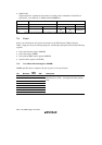
• P40/TMCI0
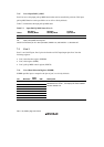
The pin function is switched as shown below according to the state of the P40DDR bit.
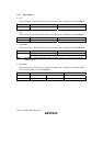
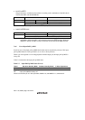
P40DDR 0 1
P40 input pin P40 output pin Pin Function
TMCI0 input pin*
Note: * When an external clock is selected with bits CKS2 to CKS0 in TCR0 of TMR_0, this pin
is used as the TMCI0 input pin.