


Rev. 1.00, 05/04, page 278 of 544
• Selectable input/output pins*
Pins, PG4/ExSDAA, PG5/ExSCLA, PG6/ExSDAB, and PG7/ExSCLB, are selectable for
the I
2
C bus input/output pin in each channel.
Note: * The program development tool (emulator) does not support this function.
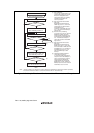
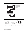
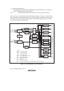
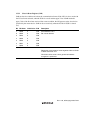
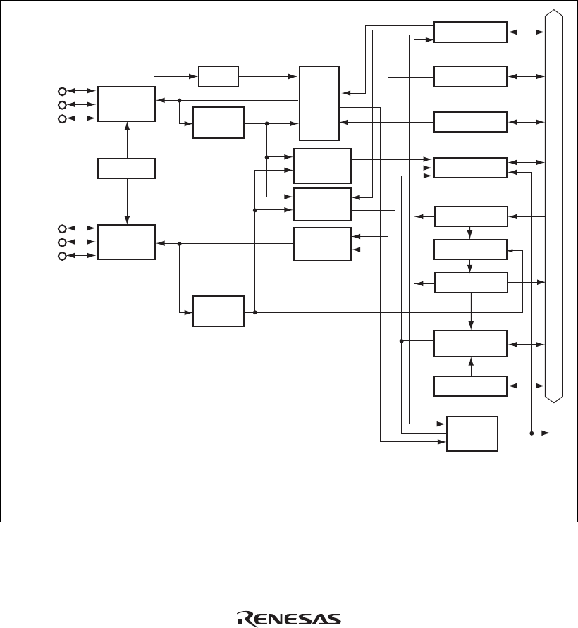
Figure 13.1 shows a block diagram of the I
2
C bus interface. Figure 13.2 shows an example of I/O
pin connections to external circuits. Since I
2
C bus interface I/O pins are different in structure from
normal port pins, they have different specifications for permissible applied voltages. For details,
see section 22, Electrical Characteristics.
φ
SCL
PS
Noise
canceler
Bus state
decision
circuit
Arbitration
decision
circuit
Output data
control
circuit
ICCR
Clock
control
ICXR
ICMR
ICSR
PGCTL
ICDRS
Address
comparator
SAR, SARX
SDA
Noise
canceler
Interrupt
generator
Interrupt
request
Internal data bus
ICDRR
ICDRT
[Legend]
ICCR:
ICMR:
ICSR:
ICDR:
ICXR:
SAR:
SARX:
PS:
PGCTL:
I
2
C bus control register
I
2
C bus mode register
I
2
C bus status register
I
2
C bus data register
I
2
C bus extended control register
Slave address register
Slave address register X
Prescaler
Port G control register
ExSCLA*
ExSCLB*
ExSDAA*
ExSDAB*
Pin
selection
circuit
Pin
selection
circuit
Note: * The program development tool (emulator) does not support this function.
Figure 13.1 Block Diagram of I
2
C Bus Interface