


Rev. 1.00, 05/04, page 56 of 544
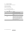
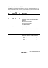
Bit Bit Name
Initial
Value R/W Description
3 FLSHE 0 R/W Flash Memory Control Register Enable
Enables or disables CPU access for flash memory
registers (FLMCR1, FLMCR2, EBR1, EBR2), control
registers in power-down state (SBYCR, LPWRCR,
MSTPCRH, MSTPCRL), and control registers of on-
chip peripheral modules (PCSR, SYSCR2).
0: Registers in power-down state and control registers
of on-chip peripheral modules are accessed in an
area from H'(FF)FF80 to H'(FF)FF87.
1: Control registers of flash memory are accessed in
an area from H'(FF)FF80 to H'(FF)FF87.
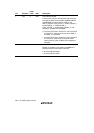
2 — 0 R/(W) Reserved
The initial value should not be changed.
1
0
ICKS1
ICKS0
0
0
R/W
R/W
Internal Clock Source Select 1, 0
These bits select a clock to be input to the timer
counter (TCNT) and a count condition together with
bits CKS2 to CKS0 in the timer control register (TCR).
For details, refer to section 10.3.4, Timer Control
Register (TCR).
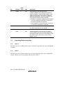
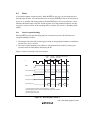
3.3 Operating Mode Descriptions
3.3.1 Mode 2
The CPU can access a 16-Mbyte address space in advanced single-chip mode. The on-chip ROM
is enabled.
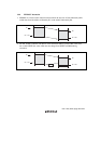
3.3.2 Mode 3
The CPU can access a 64-Kbyte address space in normal single-chip mode. The on-chip ROM is
enabled. The CPU can access a 56-kbyte address space in mode 3.