


Rev. 1.00, 05/04, page 149 of 544
8.3.1 PWM Register Select (PWSL)
PWSL is used to select the input clock and the PWM data register.
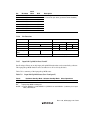
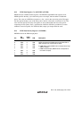
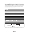
Bit Bit Name Initial Value R/W Description
7
6
PWCKE
PWCKS
0
0
R/W
R/W
PWM Clock Enable
PWM Clock Select
These bits, together with bits PWCKC, PWCKB and
PWCKA in PCSR, select the internal clock input to
TCNT in the PWM. For details, see table 8.2.
The resolution, PWM conversion period, and carrier
frequency depend on the selected internal clock, and
can be obtained from the following equations.
Resolution (minimum pulse width) = 1/internal clock
frequency
PWM conversion period = resolution × 256
Carrier frequency = 16/PWM conversion period
With a 10 MHz system clock (φ), the resolution, PWM
conversion period, and carrier frequency are as shown
in table 8.3.
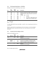
5 — 1 R Reserved
Always read as 1 and cannot be modified.
4 — 0 R Reserved
Always read as 0 and cannot be modified.
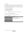
3
2
1
0
RS3
RS2
RS1
RS0
0
0
0
0
R/W
R/W
R/W
R/W
Register Select
These bits select the PWM data register.
0000: PWDR0 selected
0001: PWDR1 selected
0010: PWDR2 selected
0011: PWDR3 selected
0100: PWDR4 selected
0101: PWDR5 selected
0110: PWDR6 selected
0111: PWDR7 selected
1xxx: No effect on operation
[Legend]
x: Don't care.