


Rev. 1.00, 05/04, page 425 of 544
16.7 Usage Notes
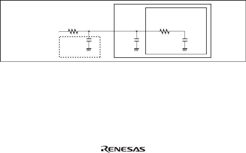
16.7.1 Permissible Signal Source Impedance
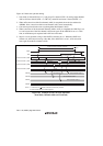
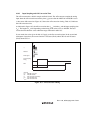
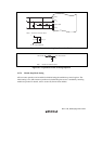
This LSI's analog input (3-V version) is designed so that the conversion accuracy is guaranteed for
an input signal for which the signal source impedance is 5 kΩ or less. This specification is
provided to enable the A/D converter's sample-and-hold circuit input capacitance to be charged
within the sampling time; if the sensor output impedance exceeds 5 kΩ, charging may be
insufficient and it may not be possible to guarantee the A/D conversion accuracy. However, if a
large capacitance is provided externally in single mode, the input load will essentially comprise
only the internal input resistance of 10 kΩ, and the signal source impedance is ignored. However,
since a low-pass filter effect is obtained in this case, it may not be possible to follow an analog
signal with a large differential coefficient (e.g., voltage fluctuation ratio of 5 mV/µs or greater)
(see figure 16.7). When converting a high-speed analog signal or converting in scan mode, a low-
impedance buffer should be inserted.
16.7.2 Influences on Absolute Accuracy
Adding capacitance results in coupling with ground, and therefore noise in ground may adversely
affect the absolute accuracy. Be sure to make the connection to an electrically stable ground such
as AVss.
Care is also required to insure that filter circuits do not communicate with digital signals on the
mounting board, so acting as antennas.
A/D converter equivalent circuit
This LSI
20 pF
C
in
=
15 pF
10 kΩ
to 5 kΩ
Low-pass
filter
C to 0.1 µF
Sensor output
impedance
Sensor input
Figure 16.7 Example of Analog Input Circuit