


Rev. 1.00, 05/04, page 447 of 544
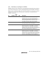
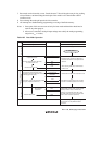
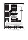
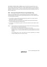
START
End of programming
Set SWE bit in FLMCR1
Start of programmingWrite pulse application subroutine
Wait (x) µs
Sub-Routine Write Pulse
End Sub
Set PSU bit in FLMCR2
WDT enable
Disable WDT
Number of Writes n
1
2
3
4
5
6
7
8
9
10
11
12
13
998
999
1000
Note 7: Write Pulse Width
Write Time (z) µs
z1
z1
z1
z1
z1
z1
z2
z2
z2
z2
z2
z2
z2
z2
z2
z2
Wait (γ) µs
Set P bit in FLMCR1
Wait (z1) µs, (z2) µs or (z3) µs
Clear P bit in FLMCR1
Wait (α) µs
Clear PSU bit in FLMCR2
Wait (β) µs
n = 1
m = 0
NG
NG
NG
NG
NG
OK
OK
OK
Wait (γ) µs
Wait (ε) µs
*
2
*
4
*
5
*
1
Wait (η) µs
Apply write pulse z1 µs or z2 µs
Sub-Routine-Call
Set PV bit in FLMCR1
H'FF dummy write to verify address
Read verify data
Write data =
verify data?
*
4
*
3
*
3
*
1
Transfer reprogram data to reprogram data area
Reprogram data computation
*
4
Transfer additional-programming data to
additional-programming data area
Additional-programming data computation
Clear PV bit in FLMCR1
Clear SWE bit in FLMCR1
m = 1
See Note 7 for pulse width
m = 0 ?
Increment address
Programming failure
OK
Clear SWE bit in FLMCR1
Wait (θ) µs
µs
OK
6 ≥ n?
NG
OK
6 ≥ n ?
Wait (θ) µs
n ≥ (N)?
n ← n + 1
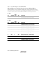
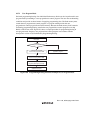
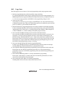
Original Data
(D)
Verify Data
(V)
Reprogram Data
(X)
Comments
Programming completed
Still in erased state; no action
Programming incomplete;
reprogram
Note:
Use a z3 µs write pulse for additional programming.
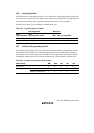
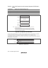
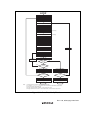
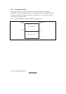
Write 128-byte data in RAM reprogram
data area consecutively to flash memory
RAM
Program data storage
area (128 bytes)
Reprogram data storage
area (128 bytes)
Additional-programming
data storage area
(128 bytes)
Store 128-byte program data in program
data area and reprogram data area
Apply write pulse (Additional programming)
128-byte
data verification completed?
Successively write 128-byte data from additional-
programming data area in RAM to flash memory
Reprogram Data Computation Table
Reprogram Data
(X')
Verify Data
(V)
Additional-
Programming Data
(Y)
1
1
1
1
0
1
0
000
1
1
Comments
Additional programming
to be executed
Additional programming
not to be executed
Additional programming
not to be executed
0
1
1
1
0
1
0
100
1
1
Additional-Programming Data Computation Table
Perform programming in the erased state.
Do not perform additional programming
on previously programmed addresses.
Notes: 1. Data transfer is performed by byte transfer. The lower 8 bits of the first address written to must be H'00 or H'80. A 128-byte data transfer must be performed even if
writing fewer than 128 bytes; in this case, H'FF data must be written to the extra addresses.
2. Verify data is read in 16-bit (word) units.
3. Even bits for which programming has been completed will be subjected to programming once again if the result of the subsequent verify operation is NG.
4. A 128-byte area for storing program data, a 128-byte area for storing reprogram data, and a 128-byte area for storing additional data must be provided in RAM.
The contents of the reprogram data area and additional data area are modified as programming proceeds.
5. A write pulse of z1 µs or z2 µs is applied according to the progress of the programming operation. See Note7 for details of the pulse widths. When writing of
additional-programming data is executed, a z3 µs write pulse should be applied. Reprogram data X' means reprogram data when the write pulse is applied.
6. The values of x, y, z1, z2, z3, α, β, γ, ε, η, θ, and N are shown in section 22.5, Flash Memory Characteristics.
Figure 18.9 Program/Program-Verify Flowchart