


Rev. 1.00, 05/04, page 518 of 544
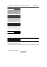
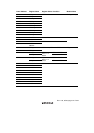
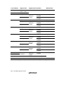
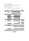
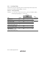
Table 22.3 Permissible Output Currents
Conditions: V
CC
= 3.0 V to 3.6 V, V
CC
B = 3.0 V to 5.5 V, V
SS
= 0 V, T
a
= –20 to +75°C
Item Symbol Min. Typ. Max. Unit
SCL1, SCL0,
SDA1, SDA0,
PS2AC to PS2CC,
PS2AD to PS2CD,
PA7 to PA4,
ExSDAA, ExSCLA,
ExSDAB, ExSCLB
(bus drive function
selected)
— — 10
Ports 1, 2, 3 — — 2
RESO — — 1
Permissible
output
low current
(per pin)
Other output pins
I
OL
— — 1
mA
Total of ports 1, 2,
and 3
— — 40 Permissible
output
low current
(total)
Total of all output
pins, including the
above
∑ I
OL
— — 60
mA
Permissible
output
high current
(per pin)
All output pins –I
OH
— — 2 mA
Permissible
output
high current
(total)
Total of all output
pins
∑ –I
OH
— — 30 mA
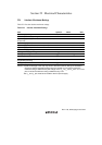
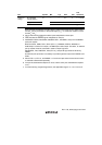
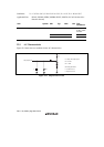
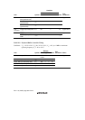
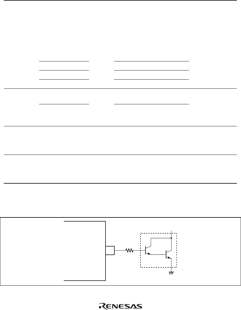
Notes: 1. To protect chip reliability, do not exceed the output current values in table 22.3.
2. When driving a Darlington pair or LED, always insert a current-limiting resistor in the
output line, as show in figures 22.1 and 22.2.
2 kΩ
This LSI
Port
Darlington pair
Figure 22.1 Darlington Pair Drive Circuit (Example)