


Rev. 1.00, 05/04, page 140 of 544
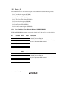
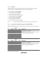
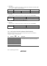
• PF2/TMOA
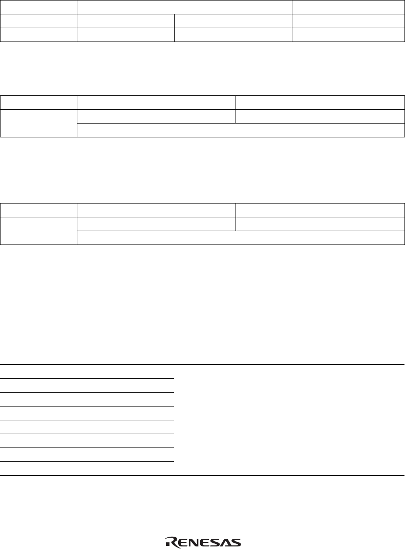
The pin function is switched as shown below according to the combination of the OS3 to OS0
bits in TCSR_A of TMR_A and the PF2DDR bit.
OS3 to OS0 All 0 Not all 0
PF3DDR 0 1 —
Pin Function PF2 input pin PF2 output pin TMOA output pin
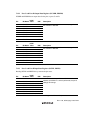
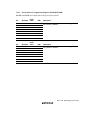
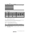
• PF1/TMIB
The pin function is switched as shown below according to the state of the PF1DDR bit.
PF1DDR 0 1
PF1 input pin PF1 output pin Pin Function
TMIB input pin*
Note: * This pin can always be used as the TMIB input pin.
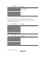
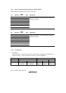
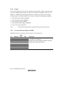
• PF0/TMIA
The pin function is switched as shown below according to the state of the PF0DDR bit.
PF0DDR 0 1
PF0 input pin PF0 output pin Pin Function
TMIA input pin*
Note: * This pin can always be used as the TMIA input pin.
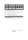
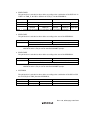
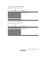
7.13.5 Port E and Port F Nch-OD Control Register (PENOCR, PFNOCR)
PENOCR and PFNOCR specify the output driver type for pins on ports E and F which are
configured as outputs on a bit-by-bit basis.
Bit Bit Name
Initial
Value
R/W Description
7 PE7NOCR 0 R/W
6 PE6NOCR 0 R/W
5 PE5NOCR 0 R/W
4 PE4NOCR 0 R/W
3 PE3NOCR 0 R/W
2 PE2NOCR 0 R/W
1 PE1NOCR 0 R/W
0 PE0NOCR 0 R/W
0: CMOS (p-channel driver enabled)
1: N-channel open drain (p-channel driver disabled)