


Rev. 1.00, 05/04, page 381 of 544
15.3.5 Output Data Registers 1 to 3 (ODR1 to ODR3)
The ODR registers are 8-bit readable/writable registers for the slave processor (this LSI), and 8-bit
read-only registers for the host processor. The registers selected from the host according to the I/O
address are shown in the following table. For information on ODR3 selection, see section 15.3.3,
LPC Channel 3 Address Register (LADR3). In an LPC I/O read cycle, the data in the selected
register is transferred to the host. The initial values of ODR1 to ODR3 are undefined.
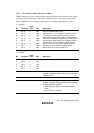
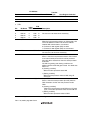
I/O Address
Bits 15 to 4 Bit 3 Bit 2 Bit 1 Bit 0
Transfer
Cycle
Host Register Selection
0000 0000 0110 0 0 0 0 I/O read ODR1 read
0000 0000 0110 0 0 1 0 I/O read ODR2 read
15.3.6 Bidirectional Data Registers 0 to 15 (TWR0 to TWR15)
The TWR registers are sixteen 8-bit readable/writable registers to both the slave processor (this
LSI) and the host processor. In TWR0, however, two registers (TWR0MW and TWR0SW) are
allocated to the same address for both the host address and the slave address. TWR0MW is a
write-only register for the host processor, and a read-only register for the slave processor, while
TWR0SW is a write-only register for the slave processor and a read-only register for the host
processor. When the host and slave processors begin a write, after the respective TWR0 registers
have been written to, access right arbitration for simultaneous access is performed by checking the
status flags to see if those writes were valid. For the registers selected from the host according to
the I/O address, see section 15.3.3, LPC Channel 3 Address Register (LADR3).
Data transferred in an LPC I/O write cycle is written to the selected register; in an LPC I/O read
cycle, the data in the selected register is transferred to the host. The initial values of TWR0 to
TWR15 are undefined.
15.3.7 Status Registers 1 to 3 (STR1 to STR3)
The STR registers are 8-bit registers that indicate status information during host interface
processing. Bits 3, 1, and 0 of STR1 to STR3, and bits 7 to 4 of STR3, are read-only bits for both
the host processor and the slave processor (this LSI). However, only 0 can be written to bit 0 of
STR1 to STR3 and bits 6 and 4 of STR3, from the slave processor (this LSI), in order to clear the
flags to 0. The registers selected from the host processor according to the I/O address are shown in
the following table. For information on STR3 selection, see section 15.3.3, LPC Channel 3
Address Register (LADR3). In an LPC I/O read cycle, the data in the selected register is
transferred to the host processor. The initial values of STR1 to STR3 are H'00.