


Rev. 1.00, 05/04, page 382 of 544
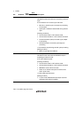
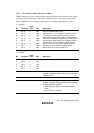
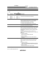
I/O Address
Bits 15 to 4 Bit 3 Bit 2 Bit 1 Bit 0
Transfer
Cycle
Host Register Selection
0000 0000 0110 0 1 0 0 I/O read STR1 read
0000 0000 0110 0 1 1 0 I/O read STR2 read
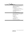
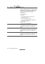
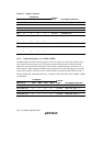
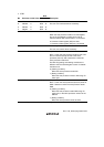
• STR1
R/W
Bit Bit Name
Initial
Value
Slave Host
Description
7
6
5
4
DBU17
DBU16
DBU15
DBU14
0
0
0
0
R/W
R/W
R/W
R/W
R
R
R
R
Defined by User
The user can use these bits as necessary.
3 C/D1 0 R R Command/Data
When the host processor writes to an IDR register, bit 2
of the I/O address is written into this bit to indicate
whether IDR contains data or a command.
0: Contents of data register (IDR) are data
1: Contents of data register (IDR) are a command
2 DBU12 0 R/W R Defined by User
The user can use this bit as necessary.
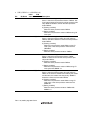
1 IBF1 0 R R Input Buffer Full
Set to 1 when the host processor writes to IDR. This bit
is an internal interrupt source to the slave processor
(this LSI). IBF is cleared to 0 when the slave processor
reads IDR.
The IBF1 flag setting and clearing conditions are
different when the fast A20 gate is used. For details see
table 15.3.
0: [Clearing condition]
When the slave processor reads IDR
1: [Setting condition]
When the host processor writes to IDR using I/O
write cycle
0 OBF1 0 R/(W)* R Output Buffer Full
Set to 1 when the slave processor (this LSI) writes to
ODR. Cleared to 0 when the host processor reads
ODR.
0: [Clearing condition]
When the host processor reads ODR using I/O read
cycle, or the slave processor writes 0 to the OBF bit
1: [Setting condition]
When the slave processor writes to ODR
Note: * Only 0 can be written to clear the flag.