


Rev. 1.00, 05/04, page 438 of 544
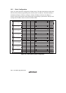
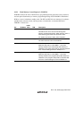
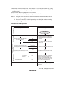
18.5.1 Flash Memory Control Register 1 (FLMCR1)
FLMCR1, used together with FLMCR2, makes the flash memory transit to program mode,
program-verify mode, erase mode, or erase-verify mode. For details on register setting, refer to
section 18.8, Flash Memory Programming/Erasing.FLMCR1 is initialized to H'80 by a reset, or in
hardware standby mode, software standby mode, sub-active mode, sub-sleep mode, or watch
mode.
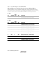
Bit Bit Name
Initial
Value R/W Description
7 FWE 1 R Flash Write Enable
Controls programming/erasing of on-chip flash
memory. This bit is always read as 0, and cannot be
modified.
6 SWE 0 R/W Software Write Enable
When this bit is set to 1, flash memory
programming/erasing is enabled. When this bit is
cleared to 0, the EV, PV, E, and P bits in this register,
the ESU and PSU bits in FLMCR2, and all EBR1 and
EBR2 bits cannot be set to 1. Do not clear these bits
and SWE to 0 simultaneously.
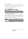
5
4
—
—
0
0
R
R
Reserved
These bits are always read as 0 and cannot be
modified.
3 EV 0 R/W Erase-Verify
When this bit is set to 1 while SWE = 1, the flash
memory transits to erase-verify mode. When it is
cleared to 0, erase-verify mode is cancelled.
2 PV 0 R/W Program-Verify
When this bit is set to 1 while SWE = 1, the flash
memory transits to program-verify mode. When it is
cleared to 0, program-verify mode is cancelled.
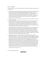
1 E 0 R/W Erase
When this bit is set to 1 while SWE = 1 and ESU = 1,
the flash memory transits to erase mode. When it is
cleared to 0, erase mode is cancelled.
0 P 0 R/W Program
When this bit is set to 1 while SWE = 1 and PSU = 1,
the flash memory transits to program mode. When it is
cleared to 0, program mode is cancelled.