


Rev. 1.00, 05/04, page 515 of 544
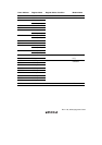
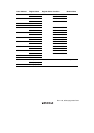
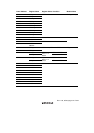
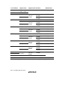
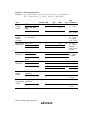
Item Symbol Min. Typ. Max. Unit
Test
Conditions
All output pins
(except RESO)*
5
— — 0.4 V I
OL
= 1.6 mA
Ports 1 to 3 — — 1.0 V I
OL
= 5 mA
Output low
voltage
RESO
V
OL
— — 0.4 V I
OL
= 1.6 mA
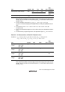
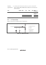
Notes: 1. Do not leave the AVcc, AVref, and AVss pins open even if the A/D converter is not used.
Even if the A/D converter is not used, apply a value in the range 2.0 V to 3.6 V to AV
CC
and AV
ref
pins by connection to the power supply (V
CC
), or some other method. Ensure
that AV
ref
≤ AV
CC
.
2. P67 to P60 include peripheral module inputs multiplexed on those pins.
3. IRQ2 includes the ADTRG signal multiplexed on that pin.
4. P52/ExSCK1/SCL0, P97/SDA0, P86/SCK1/SCL1, P42/SDA1, and port G are NMOS
push-pull outputs.
When the SCL0, SDA0, SCL1, SDA1 (ICE = 1), ExSDAA, ExSCLA, ExSDAB, or
ExSCLB pin is used as an output, it is NMOS open-drain output. Therefore, an external
pull-up resistor must be connected in order to output high level.
P52/ExSCK1, P97, P86/SCK1, P42 (ICE = 0), and port G high levels are driven by
NMOS.
An external pull-up resistor is necessary to provide high-level output from ExSCK1 and
SCK1.
5. When IICS = 0, ICE = 0, and KBIOE = 0. Low-level output when the bus drive function
is selected is determined separately.
6. The port A characteristics depend on V
CC
B, and the other pins characteristics depend
on V
CC
.
7. For flash memory programming/erasure, the applicable range is V
CC
= 3.0 V to 3.6 V.