Rev. 1.00, 05/04, page 459 of 544
t
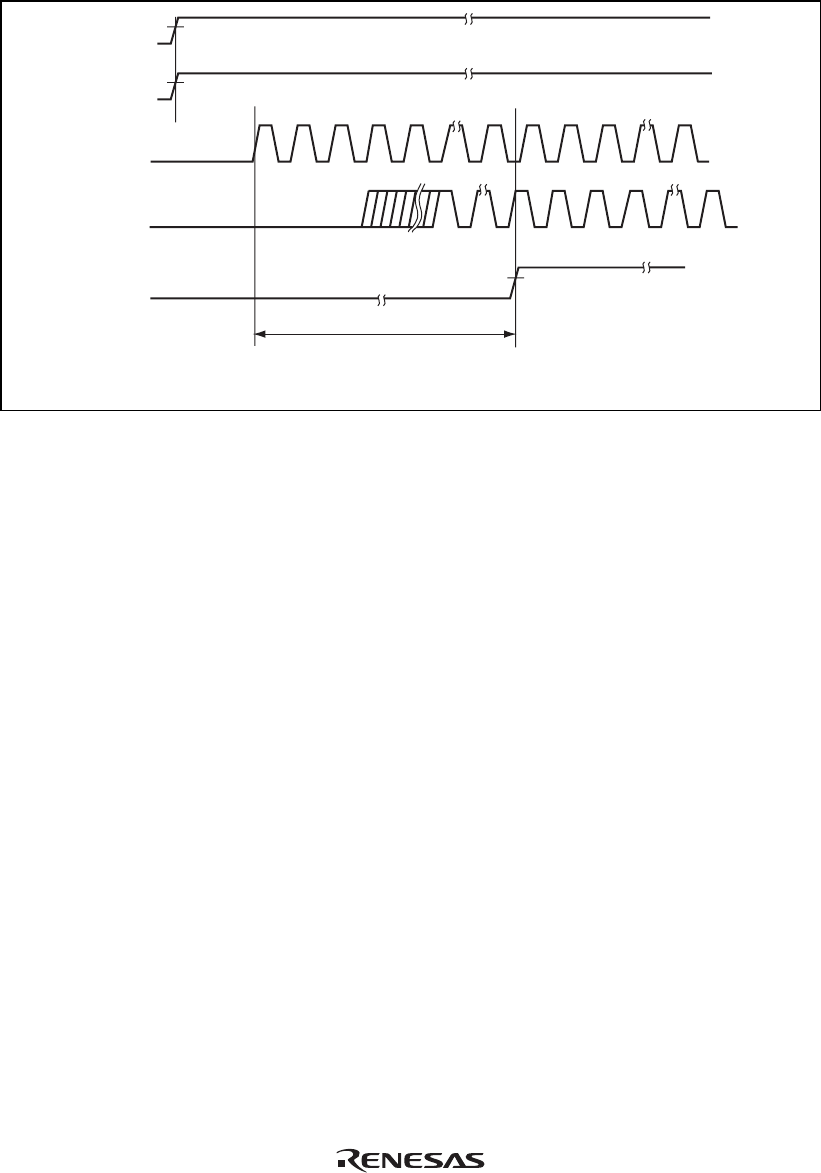
DEXT
*
RES
(Internal and external)
EXTAL
STBY
V
CC
3.0 V
V
IH
φ
Note: * The external clock output stabilization delay time (t
DEXT
) includes a RES pulse width (t
RESW
).
Figure 19.6 Timing of External Clock Output Stabilization Delay Time
19.2 Duty Correction Circuit
The duty correction circuit is valid when the oscillating frequency is 5 MHz or more. It corrects
the duty of a clock that is output from the oscillator, and generates the system clock (φ).
19.3 Medium-Speed Clock Divider
The medium-speed clock divider divides the system clock (φ), and generates φ/2, φ/4, φ/8, φ/16,
and φ/32 clocks.
19.4 Bus Master Clock Select Circuit
The bus master clock select circuit selects a clock to supply the bus master with either the system
clock (φ) or medium-speed clock (φ/2, φ/4, φ/8, φ/16, or φ/32) by the SCK2 to SCK0 bits in
SBYCR.


