


Rev. 1.00, 05/04, page 455 of 544
Section 19 Clock Pulse Generator
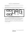
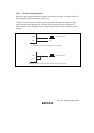
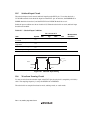
This LSI incorporates a clock pulse generator, which generates the system clock (φ), bus master
clock, and internal clock.
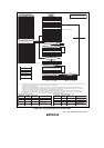
The clock pulse generator consists of an oscillator, duty correction circuit, clock select circuit,
medium-speed clock divider, bus master clock select circuit, subclock input circuit, and waveform
forming circuit. Figure 19.1 shows a block diagram of the clock pulse generator.
Oscillator
Duty
correction
circuit
Clock select
circuit
Medium-
speed clock
divider
Bus master
clock select
circuit
Subclock
input circuit
Waveform
forming
circuit
EXTAL
XTAL
EXCL
φ/2
to φ/32
φSUB
φ
WDT_1
count clock
System clock
to φ pin
Internal clock
to peripheral
modules
Bus master cloc
k
to CPU
Figure 19.1 Block Diagram of Clock Pulse Generator
The bus master clock is selected as either high-speed mode or medium-speed mode by software
according to the settings of the SCK2 to SCK0 bits in the standby control register. For details on
the standby control register, refer to section 20.1.1, Standby Control Register (SBYCR).
The subclock input is controlled by software according to the EXCLE bit setting in the low power
control register. For details on the low power control register, refer to section 20.1.2, Low Power
Control Register (LPWRCR).