


Rev. 1.00, 05/04, page 9 of 544
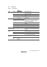
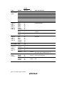
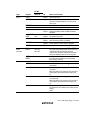
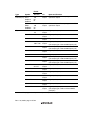
1.3.3 Pin Functions
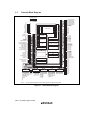
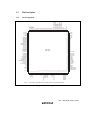
Table 1.2 Pin Functions
Pin No.
Type Symbol TFP-144 I/O Name and Function
VCC 1, 86 Input Power supply pin. Connect the pin to the
system power supply.
VCL 13 Input Power supply pin. Connect the pin to VCC.
VCCB 36 Input The power supply for the port A input/output
buffer.
Power
VSS 7, 42, 95,
111, 139
Input Ground pin. Connect to the system power
supply (0 V).
XTAL 143 Input
EXTAL 144 Input
Pins for connection to crystal resonators. The
EXTAL pin can also input an external clock.
See section 19, Clock Pulse Generator, for
typical connection diagrams.
φ 18 Output Supplies the system clock to external
devices.
EXCL 18 Input Input a 32.768 kHz external subclock.
X1 140 Input Leave open.
Clock
X2 141 Input Leave open.
Operating
mode control
MD1
MD0
9
10
Input These pins set the operating mode. These
pins should not be changed while the MCU is
operating.
RES 8 Input Reset pin.
When this pin becomes low, the chip is reset.
RESO 142 Output Outputs reset signal to external device.
System
control
STBY 12 Input When this pin is driven low, a transition is
made to hardware standby mode.
NMI
11 Input Input pin for a nonmaskable interrupt request.Interrupt
signals
IRQ0 to
IRQ7
22 to 24,
133 to 135,
84, 85
Input These pins request a maskable interrupt.