


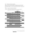
Rev. 1.00, 05/04, page 516 of 544
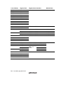
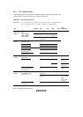
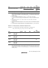
Table 22.2 DC Characteristics (2)
Conditions: V
CC
= 3.0 V to 3.6 V*
5
, V
CC
B = 3.0 V to 5.5 V, AV
CC
*
1
= 3.0 V to 3.6 V,
AV
ref
*
1
= 3.0 V to AV
CC
, V
SS
= AV
SS
*
1
= 0 V, T
a
= –20 to +75°C
Item Symbol Min. Typ. Max. Unit
Test
Conditions
RES — — 10.0
STBY, NMI, MD1,
MD0
— — 1.0
V
in
= 0.5 to
V
CC
– 0.5 V
Input
leakage
current
Port 7
I
in
— — 1.0
µA
V
in
= 0.5 to
AV
CC
– 0.5 V
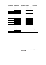
Three-state
leakage
current
(off state)
Ports 1 to 6, 8, 9,
A*
4
, and B to G
I
TSI
— — 1.0 µA V
in
= 0.5 to
V
CC
– 0.5 V,
V
in
= 0.5 to
V
CC
B – 0.5 V
Ports 1 to 3 5 — 150
Ports 6 and B to F 30 — 300
Input pull-up
MOS current
Ports A*
4
–I
P
30 — 600
µA V
in
= 0 V,
V
CC
= 3.0 V
to 3.6 V
V
CC
B = 3.0 V
to 5.5 V
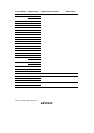
RES — — 80 pF
NMI
(4)
— — 50 pF
Input
capacitance
Input pins except (4)
above
C
in
— — 10 pF
V
in
= 0 V,
f = 1 MHz,
T
a
= 25°C
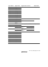
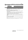
Normal operation — 30 40 mA f = 10 MHz
Sleep mode — 20 32 mA f = 10 MHz
— 1 5.0 T
a
≤ 50°C
Current
dissipation*
2
Standby mode*
3
I
CC
— — 20.0
µA
50°C < T
a
During A/D
conversion
— 1.2 2.0 mA Analog power
supply
current
Idle
Al
CC
— 0.01 5.0 µA AV
CC
= 2.0 V
to 3.6 V
During A/D
conversion
— 0.5 1.0 mA Reference
power supply
current
Idle
Al
ref
— 0.01 5.0 µA AV
ref
= 2.0 V
to AV
CC