


Rev. 1.00, 05/04, page 111 of 544
7.5.3 Pin Functions
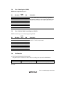
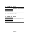
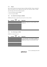
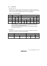
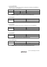
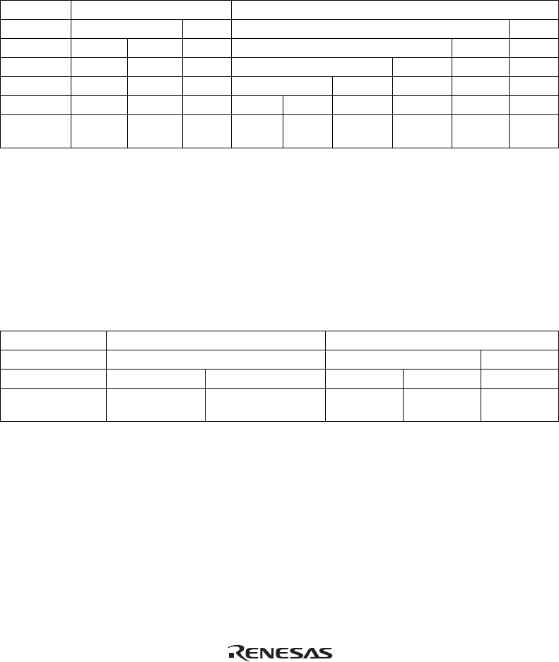
• P52/ExSCK1*/SCL0
The pin function is switched as shown below according to the combination of the C/A bit in
SMR of SCI_1, the CKE0 and CKE1 bits in SCR, the SPS1 bit*
1
in SPSR, the ICE bit in ICCR
of IIC_0, the IIC0AS and the IIC0BS bits in PGCTL*
2
, and the P52DDR bit.
P52ICE = ICE • (IIC0AS+IIC0BS)*
2
SPS1*
1
0 1
P52ICE*
2
0 1 0 1
CKE1 — — — 0 1 0
C/A — — — 0 1 — 0
CKE0 — — — 0 1 — — 0
P52DDR 0 1 — 0 1 — — — —
Pin Function P52
input pin
P52
output pin
SCL0
I/O pin
P52
input pin
P52
output pin
ExSCK1*
1
output pin
ExSCK1*
1
output pin
ExSCK1*
1
input pin
SCL0
I/O pin
Note: 1. When this pin is used as the SCL0 I/O pin by setting 1 to the SPS1 bit of SPSR, the bits
CKE1 and CKE0 in SCR of SCI_1 and the C/A bit in SMR must all be cleared to 0.
SCL0 is an NMOS open-drain output. When set as the P52 output pin or ExSCK1
output pin, this pin is an NMOS push-pull output.
2. The program development tool (emulator) does not support the function of PGCTL.
Thus P52ICE is treated as ICE.
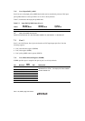
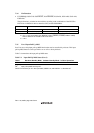
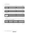
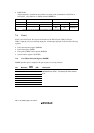
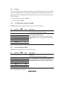
• P51/ExRxD1
The pin function is switched as shown below according to the combination of the RE bit in
SCR of SCI_1, the SPS1 bit* in SPSR, and the P51DDR bit.
SPS1* 0 1
RE — 0 1
P51DDR 0 1 0 1 —
Pin Function P51 input pin P51 output pin P51 input
pin
P51 output
pin
ExRxD1
input pin*
Note: * The program development tool (emulator) does not support this function.