


Rev. 1.00, 05/04, page 55 of 544
3.2.3 Serial Timer Control Register (STCR)
STCR enables or disables register access, IIC operating mode, and on-chip flash memory, and
selects the input clock of the timer counter.
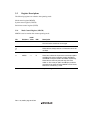
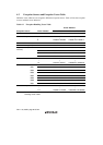
Bit Bit Name
Initial
Value R/W Description
7 IICS 0 R/W I
2
C Extra Buffer Select
Specifies bits 7 to 4 of port A as output buffers similar
to SLC and SDA. These pins are used to implement
an I
2
C interface only by software.
0: PA7 to PA4 are normal input/output pins.
1: PA7 to PA4 are input/output pins enabling bus
driving.
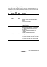
6
5
IICX1
IICX0
0
0
R/W
R/W
I
2
C Transfer Rate Select 1 and 0
These bits control the IIC operation. These bits select
a transfer rate in master mode together with bits
CKS2 to CKS0 in the I
2
C bus mode register (ICMR).
For details on the transfer rate, refer to table 13.3.
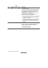
4 IICE 0 R/W I
2
C Master Enable
Enables or disables CPU access for IIC registers
(ICCR, ICSR, ICDR/SARX, ICMR/SAR), and SCI
registers (SMR, BRR, SCMR).
0: SCI_1 registers are accessed in an area from
H'(FF)FF88 to H'(FF)FF89 and from H'(FF)FF8E to
H'(FF)FF8F.
1: IIC_1 registers are accessed in an area from
H'(FF)FF88 to H'(FF)FF89 and from H'(FF)FF8E to
H'(FF)FF8F.
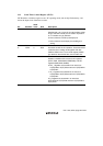
IIC_0 registers are accessed in an area from
H'(FF)FFD8 to H'(FF)FFD9 and from H'(FF)FFDE to
H'(FF)FFDF.