


Rev. 1.00, 05/04, page 11 of 544
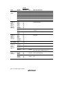
Pin No.
Type Symbol TFP-144 I/O Name and Function
LAD3 to
LAD0
124 to 121 Input/
Output
LPC command, address, and data
input/output pins.
LFRAME 125 Input Input pin that indicates the start of an LPC
cycle or forced termination of an abnormal
LPC cycle.
LRESET 126 Input Input pin that indicates an LPC reset.
LCLK 127 Input The LPC clock input pin.
SERIRQ 128 Input/
Output
Input/output pin for LPC serialized host
interrupts (HIRQ1, SMI, HIRQ6, HIRQ9 to
HIRQ12).
LSCI, LSMI,
PME
119, 120,
129
Input/
Output
LPC auxiliary output pins. Functionally, they
are general I/O ports.
GA20 130 Input/
Output
A20 gate control signal output pin. Output
state monitoring input is possible.
CLKRUN 131 Input/
Output
Input/output pin that requests the start of
LCLK operation when LCLK is stopped.
Host interface
(LPC)
LPCPD 132 Input Input pin that controls LPC module shutdown.
KIN0 to
KIN15
78 to 85,
41 to 37,
35 to 33
Input Matrix keyboard input pins. KIN0 to KIN15
are used as key-scan inputs, and P10 to P17
and P20 to P27 are used as key-scan
outputs. This allows a maximum 16-output ×
16-input, 256-key matrix to be configured.
Keyboard
buffer
controller
WUE0 to
WUE7
120 to 113 Input Wakeup event input pins. These pins allow
the same kind of wakeup as key-wakeup
from various sources.
AN5 to AN0 73 to 68 Input Analog input pins.
ADTRG 24 Input Pin for input of an external trigger to start A/D
conversion.
AVCC 76 Input The analog power supply pin for the A/D
converter.
When the A/D is not used, this pin should be
connected to the system power supply (+3
V).
AVref 77 Input The reference power supply pin for the A/D
converter and.
When the A/D is not used, this pin should be
connected to the system power supply (+3
V).
A/D converter
AVSS 67 Input The ground pin for the A/D converter. This
pin should be connected to the system power
supply
(0 V).