


Rev. 1.00, 05/04, page 517 of 544
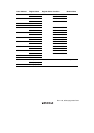
Item Symbol Min. Typ. Max. Unit
Test
Conditions
3.0 — 3.6 Operating
Analog power supply voltage*
1
AV
CC
2.0 — 3.6
V
Idle/not
used
RAM standby voltage V
RAM
2.0 — — V
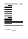
Notes: 1. Do not leave the AV
CC
, AV
ref
, and AV
SS
pins open even if the A/D converter is not used.
Even if the A/D converter is not used, apply a value in the range 2.0 V to 3.6 V to AV
CC
and AV
ref
pins by connection to the power supply (V
CC
), or some other method. Ensure
that AV
ref
≤ AV
CC
.
2. Current dissipation values are for V
IH
min = V
CC
– 0.2 V, V
CC
B – 0.2 V, and
V
IL
max = 0.2 V with all output pins unloaded and the on-chip pull-up MOSs in the off
state.
3. The values are for V
RAM
≤ V
CC
< 3.0 V, V
IH
min = V
CC
– 0.2 V, V
CC
B – 0.2 V, and
V
IL
max = 0.2 V.
4. The port A characteristics depend on V
CC
B, and the other pins characteristics depend
on V
CC
.
5. For flash memory programming/erasure, the applicable range is V
CC
= 3.0 V to 3.6 V.
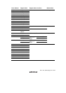
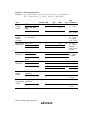
Table 22.2 DC Characteristics (3) When LPC Function is Used
Conditions: V
CC
= 3.0 V to 3.6 V, V
CC
B = 3.0 V to 5.5 V, AV
CC
* = 3.0 V to 3.6 V,
AV
ref
* = 3.0 V to AV
CC
, V
SS
= AV
SS
*
1
= 0 V, T
a
= –20 to +75°C
Item Symbol Min. Max. Unit
Test
Conditions
Input high
voltage
P37 to P30,
P83 to P80,
PB1, PB0
V
IH
V
CC
× 0.5 — V
Input low
voltage
P37 to P30,
P83 to P80,
PB1, PB0
V
IL
— V
CC
× 0.3 V
Output high
voltage
P37, P33 to P30,
P82 to P80,
PB1, PB0
V
OH
V
CC
× 0.9 — V I
OH
= –0.5
mA
Output low
voltage
P37, P33 to P30,
P82 to P80,
PB1, PB0
V
OL
— V
CC
× 0.1 V I
OL
= 1.5 mA
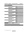
Note: * Do not leave the AV
CC
, AV
ref
, and AV
SS
pins open even if the A/D converter is not used.
Even if the A/D converter is not used, apply a value in the range 2.0 V to 3.6 V to AV
CC
and AV
ref
pins by connection to the power supply (V
CC
), or some other method. Ensure
that AV
ref
≤ AV
CC
.