


IFKEY10A_000020020700 Rev. 1.00, 05/04, page 349 of 544
Section 14 Keyboard Buffer Controller
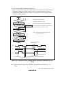
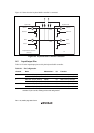
This LSI has three on-chip keyboard buffer controller channels. The keyboard buffer controller is
provided with functions conforming to the PS/2 interface specifications.
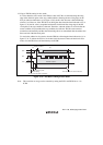
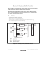
Data transfer using the keyboard buffer controller employs a data line (KD) and a clock line
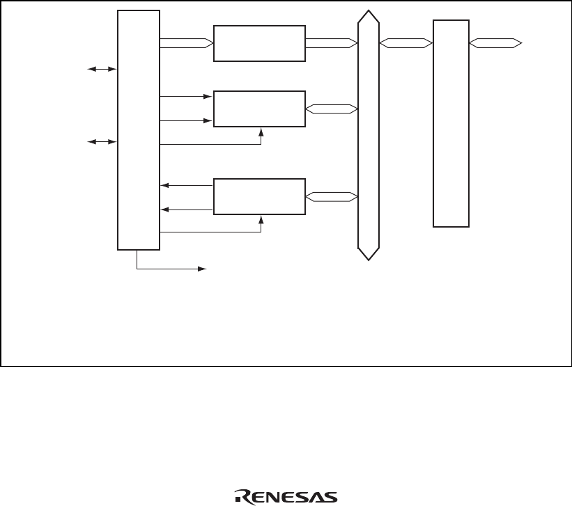
(KCLK), providing economical use of connectors, board surface area, etc. Figure 14.1 shows a
block diagram of the keyboard buffer controller.
14.1 Features
• Conforms to PS/2 interface specifications
• Direct bus drive (via the KCLK and KD pins)
• Interrupt sources: on completion of data reception and on detection of clock edge
• Error detection: parity error and stop bit monitoring
KD
(PS2AD,
PS2BD,
PS2CD)
KDI
KCLKI
KDO
KCLKO
Parity
Register counter value
KBI interrupt
KCLK
(PS2AC,
PS2BC,
PS2CC)
[Legend]
KD: KBC data I/O pin
KCLK: KBC clock I/O pin
KBBR: Keyboard data buffer register
KBCRH: Keyboard control register H
KBCRL: Keyboard control register L
Control
logic
KBBR
KBCRH
KBCRL
Bus interface
Internal
data bus
Module data bus
Figure 14.1 Block Diagram of Keyboard Buffer Controller