


Rev. 1.00, 05/04, page 130 of 544
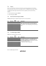
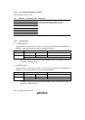
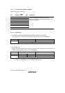
7.11.3 Port B Input Data Register (PBPIN)
PBPIN indicates the port B state.
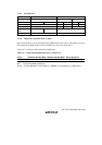
Bit Bit Name
Initial
Value R/W Description
7 PB7PIN Undefined* R
6 PB6PIN Undefined* R
5 PB5PIN Undefined* R
4 PB4PIN Undefined* R
3 PB3PIN Undefined* R
2 PB2PIN Undefined* R
1 PB1PIN Undefined* R
0 PB0PIN Undefined* R
Reading PBPIN always returns the pin states. PBPIN
has the same address as P8DDR. If a write is
performed, data will be written to P8DDR and the port
8 settings will change.
Note: * The initial value is determined according to the PB7 to PB0 pin states.
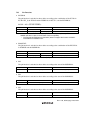
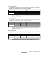
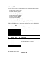
7.11.4 Pin Functions
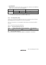
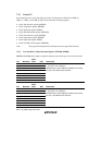
• PB7/WUE7, PB6/WUE6, PB5/WUE5, PB4/WUE4, PB3/WUE3, PB2/WUE2
The pin function is switched as shown below according to the state of the PBnDDR bit.
PBnDDR 0 1
PBn input pin PBn output pin Pin Function
WUEn input pin*
Note: * This pin can always be used as the WUEn input pin. (n = 7 to 2)
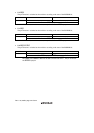
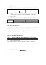
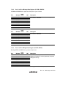
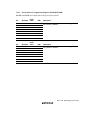
• PB1/WUE1/LSCI
The pin function is switched as shown below according to the combination of the LSCIE bit in
HICR0 of the host interface (LPC) and the PB1DDR bit.
LSCIE 0 1
PB1DDR 0 1 0*
1
PB1input pin PB1 output pin LSCI output pin Pin Function
WUE1 input pin*
2
, LSCI input pin*
2
Notes: 1. When the LSCIE bit in HICR0 is set to 1, the PB1DDR bit should be cleared to 0.
2. This pin can always be used as the WUE1 or LSCI input pin.