


Rev. 1.00, 05/04, page 523 of 544
22.3.3 Timing of On-Chip Peripheral Modules
Tables 22.7 to 22.10 show the on-chip peripheral module timing. The only on-chip peripheral
modules that can operate in subclock operation (φ = 32.768 kHz) are the I/O ports, external
interrupts (NMI and IRQ0, 1, 2, 6, and 7), the watchdog timer, and the 8-bit timer (channels 0 and
1).
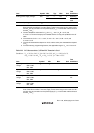
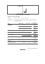
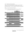
Table 22.7 Timing of On-Chip Peripheral Modules (1)
Conditions: V
CC
= 3.0 V to 3.6 V, V
CC
B = 3.0 V to 5.5 V, V
SS
= 0 V, φ = 32.768 kHz
*
,
4 MHz to maximum operating frequency, T
a
= –20 to +75°C
Condition
10 MHz
Item Symbol
Min. Max.
Unit
Test
Conditions
Output data delay time t
PWD
— 100
Input data setup time t
PRS
50 —
I/O ports
Input data hold time t
PRH
50 —
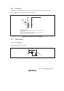
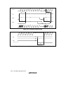
ns Figure 22.10
Timer output delay time t
FTOD
— 100
Timer input setup time t
FTIS
50 —
Figure 22.11
Timer clock input setup time t
FTCS
50 —
ns
Single edge t
FTCWH
1.5 —
FRT
Timer clock
pulse width
Both edges
t
FTCWL
2.5 —
t
cyc
Figure 22.12
Timer output delay time t
TMOD
— 100 Figure 22.13
Timer reset input setup time t
TMRS
50 — Figure 22.15
Timer clock input setup time t
TMCS
50 —
ns
Single edge t
TMCWH
1.5 —
TMR
Timer clock
pulse width
Both edges
t
TMCWL
2.5 —
t
cyc
Figure 22.14
PWM Pulse output delay time t
PWOD
— 100 ns Figure 22.16
Asynchronous t
Scyc
4 — Input clock
cycle
Synchronous
6 —
t
cyc
Input clock pulse width t
SCKW
0.4 0.6 t
Scyc
Input clock rise time t
SCKr
— 1.5
SCI
Input clock fall time t
SCKf
— 1.5
t
cyc
Figure 22.17