


Rev. 1.00, 05/04, page 269 of 544
Yes
<End>
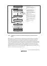
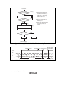
[1]
No
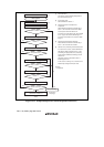
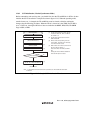
Initialization
Start reception
[2]
No
Yes
Read RDRF flag in SSR [4]
[5]
Clear RE bit in SCR to 0
Error processing
(Continued below)
[3]
Read receive data in RDR and
clear RDRF flag in SSR to 0
No
Yes
ORER = 1
RDRF = 1
All data received?
Read ORER flag in SSR
<End>
Error processing
Overrun error processing
Clear ORER flag in SSR to 0
[3]
[1] SCI initialization:
The RxD pin is automatically
designated as the receive data input
pin.
[2] [3] Receive error processing:
If a receive error occurs, read the
ORER flag in SSR, and after
performing the appropriate error
processing, clear the ORER flag to 0.
Transfer cannot be resumed if the
ORER flag is set to 1.
[4] SCI status check and receive data
read:
Read SSR and check that the RDRF
flag is set to 1, then read the receive
data in RDR and clear the RDRF flag
to 0.
Transition of the RDRF flag from 0 to
1 can also be identified by an RXI
interrupt.
[5] Serial reception continuation
procedure:
Figure 12.19 Sample Serial Reception Flowchart
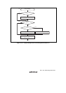
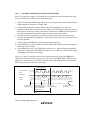
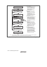
12.6.5 Simultaneous Serial Data Transmission and Reception (Clocked Synchronous
Mode)
Figure 12.20 shows a sample flowchart for simultaneous serial transmit and receive operations.
After initializing the SCI, the following procedure should be used for simultaneous serial data
transmit and receive operations. To switch from transmit mode to simultaneous transmit and
receive mode, check that the SCI has finished transmission and the TDRE and TEND flags in SSR
are set to 1, clear the TE bit in SCR to 0, and then set the TE and RE bits to 1 simultaneously with
a single instruction. To switch from receive mode to simultaneous transmit and receive mode,
check that the SCI has finished reception, and clear the RE bit to 0. Then after checking that the
RDRF bit in SSR and receive error flags (ORER, FER, and PER) are cleared to 0, set the TE and
RE bits to 1 simultaneously with a single instruction.