


Rev. 1.00, 05/04, page 262 of 544
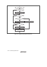
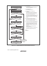
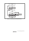
Yes
<End>
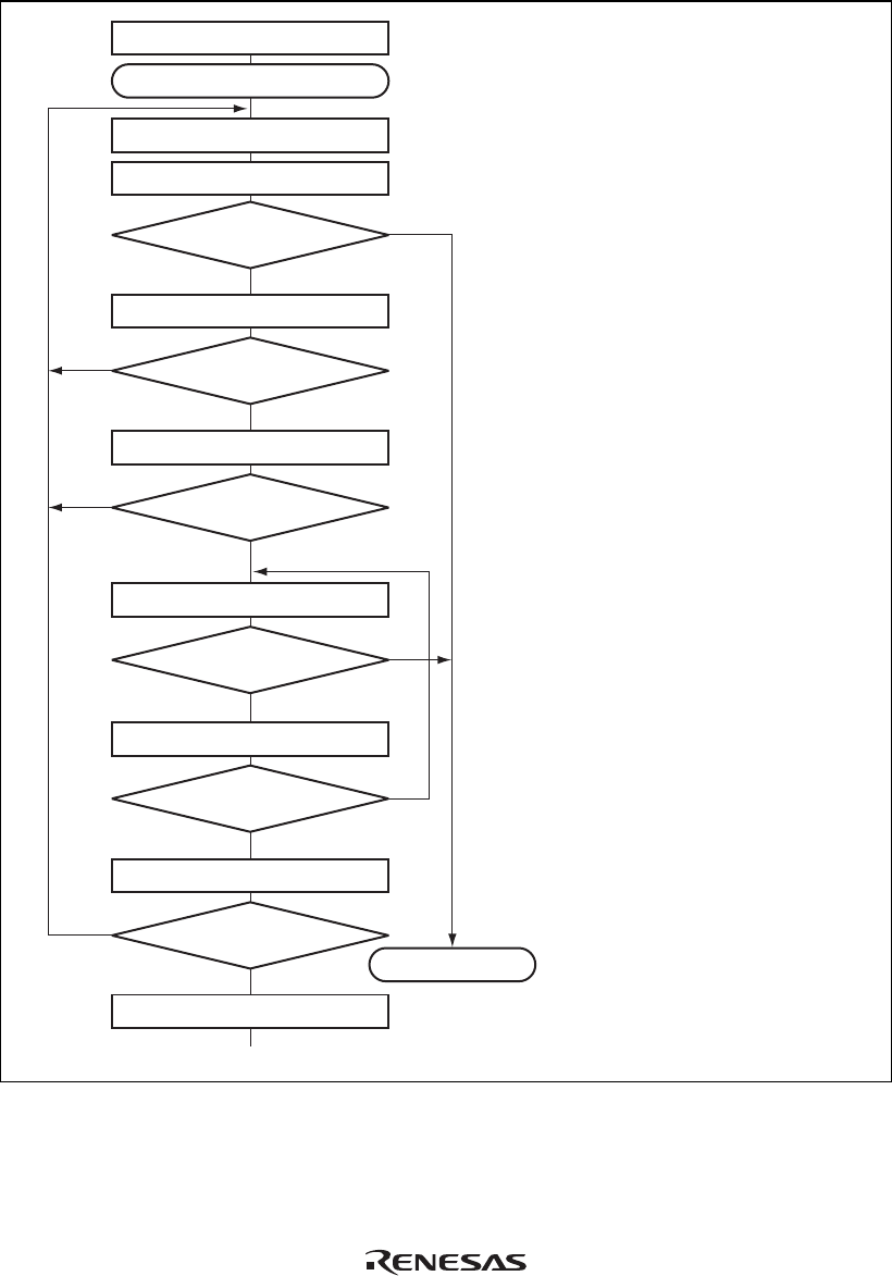
[1]
No
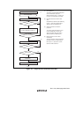
Initialization
Start reception
No
Yes
[4]
Clear RE bit in SCR to 0
Error processing
(Continued on
next page)
[5]
No
Yes
FER ∨ ORER = 1
RDRF = 1
All data received?
Set MPIE bit in SCR to 1 [2]
Read ORER and FER flags in SSR
Read RDRF flag in SSR [3]
Read receive data in RDR
No
Yes
This station’s ID?
Read ORER and FER flags in SSR
Yes
No
Read RDRF flag in SSR
No
Yes
FER ∨ ORER = 1
Read receive data in RDR
RDRF = 1
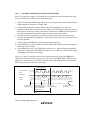
[1] SCI initialization:
The RxD pin is automatically designated as
the receive data input pin.
[2] ID reception cycle:
Set the MPIE bit in SCR to 1.
[3] SCI status check, ID reception and
comparison:
Read SSR and check that the RDRF flag is
set to 1, then read the receive data in RDR
and compare it with this station’s ID.
If the data is not this station’s ID, set the MPIE
bit to 1 again, and clear the RDRF flag to 0.
If the data is this station’s ID, clear the RDRF
flag to 0.
[4] SCI status check and data reception:
Read SSR and check that the RDRF flag is
set to 1, then read the data in RDR.
[5] Receive error processing and break detection:
If a receive error occurs, read the ORER and
FER flags in SSR to identify the error. After
performing the appropriate error processing,
ensure that the ORER and FER flags are all
cleared to 0.
Reception cannot be resumed if either of
these flags is set to 1.
In the case of a framing error, a break can be
detected by reading the RxD pin value.
[Legend]
∨ : Logical OR
Figure 12.13 Sample Multiprocessor Serial Reception Flowchart (1)