


Rev. 1.00, 05/04, page 120 of 544
• P84/IRQ3/TxD1
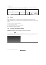
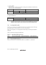
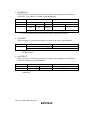
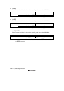
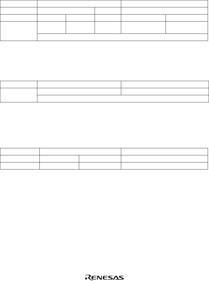
The pin function is switched as shown below according to the combination of the TE bit in
SCR of SCI_1, the SPS1 bit*
2
in SPSR, and the P84DDR bit.
SPS1*
2
0 1
TE 0 1 —
P84DDR 0 1 — 0 1
P84 input
pin
P84 output
pin
TxD1
output pin
P84 input pin P84 output pin Pin Function
IRQ3 input pin*
1
Notes: 1. When the IRQ3E bit in IER is set to 1, this pin is used as the IRQ3 input pin.
2. The program development tool (emulator) does not support this function.
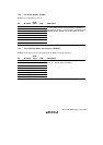
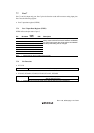
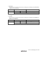
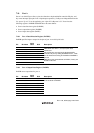
• P83/LPCPD
The pin function is switched as shown below according to the state of the P83DDR bit.
P83DDR 0 1
P83 input pin P83 output pin Pin Function
LPCPD input pin*
Note: * When at least one of bits LPC3E to LPC1E is set to 1 in HICR0, this pin is used as the
LPCPD input pin.
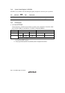
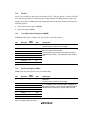
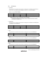
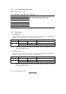
• P82/CLKRUN
The pin function is switched as shown below according to the combination of the LPC3E to
LPC1E bits in HICR0, and the P82DDR bit.
LPC3E to LPC1E All 0 Not all 0
P82DDR 0 1 0*
Pin Function P82 input pin P82 output pin CLKRUN I/O pin
Note: * When at least one of bits LPC3E to LPC1E is set to 1in HICR0, the P82DDR should be
cleared to 0.