


Rev. 1.00, 05/04, page 513 of 544
Section 22 Electrical Characteristics
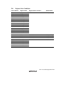
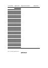
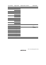
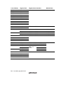
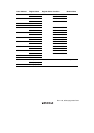
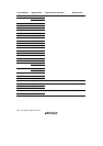
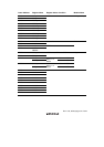
22.1 Absolute Maximum Ratings
Table 22.1 lists the absolute maximum ratings.
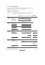
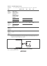
Table 22.1 Absolute Maximum Ratings
Item Symbol Value Unit
Power supply voltage V
CC
, V
CL
–0.3 to +4.3 V
I/O buffer power supply voltage V
CC
B –0.3 to +7.0 V
Input voltage (except ports 7, A, P97, P86, P52, P42,
and port G)
V
in
–0.3 to V
CC
+0.3 V
Input Voltage (port A) V
in
–0.3 to V
CC
B +0.3 V
Input voltage (P97, P86, P52, P42 and port G) V
in
–0.3 to +7.0 V
Input voltage (port 7) V
in
–0.3 to AV
CC
+ 0.3 V
Reference supply voltage AV
ref
–0.3 to AV
CC
+ 0.3 V
Analog power supply voltage AV
CC
–0.3 to +4.3 V
Analog input voltage V
AN
–0.3 to AV
CC
+0.3 V
Operating temperature T
opr
–20 to +75 °C
Operating temperature (flash memory
programming/erasing)
T
opr
–20 to +75 °C
Storage temperature T
stg
–55 to +125 °C
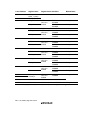
Caution: Permanent damage to the chip may result if absolute maximum ratings are exceeded.
Ensure so that the impressed voltage does not exceed 4.3 V for pins for which the
maximum rating is determined by the voltage on the V
CC
, AV
CC
, and V
CL
pins, or 7.0 V for
pins for which the maximum rating is determined by V
CC
B.
The V
CC
and V
CL
pins must be connected to the Vcc power supply.