Rev. 1.00, 05/04, page 361 of 544
14.4.4 KCLKI and KDI Read Timing
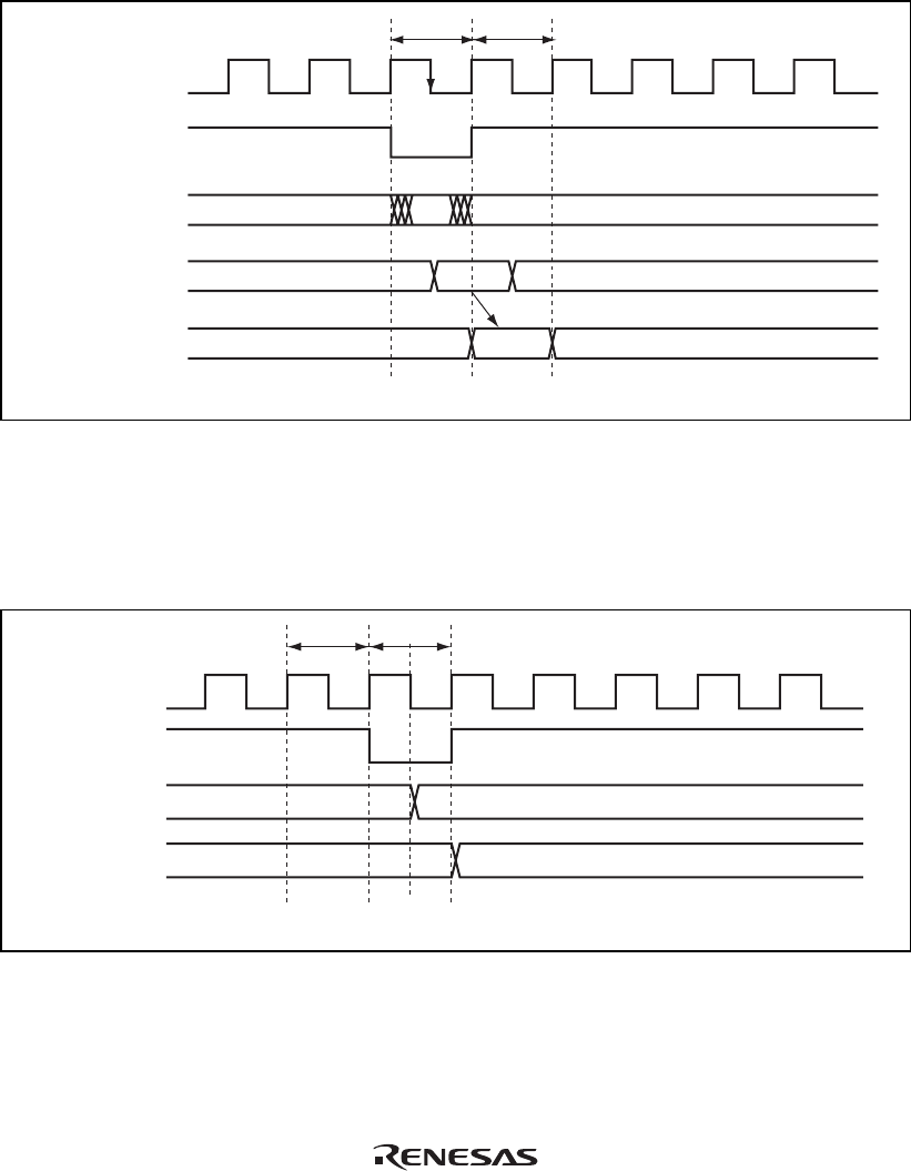
Figure 14.9 shows the KCLKI and KDI read timing.
T
1
T
2
φ
*
Internal read
signal
KCLK, KD
(pin state)
KCLKI, KDI
(register)
Internal data bus
(read data)
Note:
* The
φ
clock shown here is scaled by 1/N in medium-speed mode when the operating mode is active mode.
Figure 14.9 KCLKI and KDI Read Timing
14.4.5 KCLKO and KDO Write Timing
Figure 14.10 shows the KLCKO and KDO write timing and the KCLK and KD pin states.
Internal write
signal
φ
*
KCLKO, KDO
(register)
KCLK, KD
(pin state)
Note: * The
φ
clock shown here is scaled by 1/N in medium-speed mode when the operating mode is active mode.
T
1
T
2
Figure 14.10 KCLKO and KDO Write Timing


