AMD Geode™ SC2200 Processor Data Book 123
SuperI/O Module
32580B
5.6.2 SWC Registers
The SWC registers are organized in two banks. The offsets
are related to a base address that is determined by the
SWC Base Address Register in the logical device configu-
ration. The lower three registers are common to the two
banks while the upper registers (03h-0Fh) are divided as
follows:
• Bank 0 holds reserved registers.
• Bank 1 holds the CEIR Control Registers.
The active bank is selected through the Configuration Bank
Select field (bits [1:0]) in the Wakeup Configuration Regis-
ter (WKCFG). See Table 5-29 on page 125.
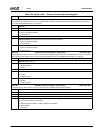
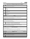
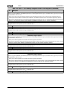
The tables that follow provide register maps and bit defini-
tions for Banks 0 and 1.
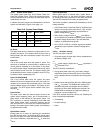
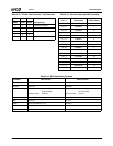
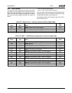
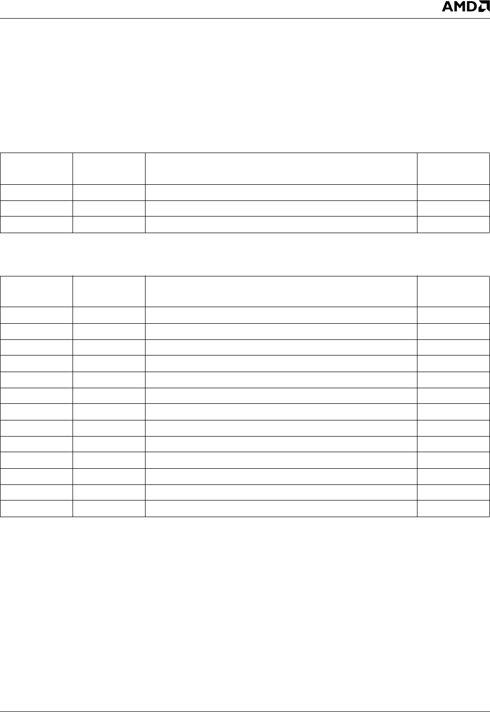
Table 5-27. Banks 0 and 1 - Common Control and Status Register Map
Offset Type Name
Reset
Value
00h R/W1C WKSR. Wakeup Events Status Register 00h
01h R/W WKCR. Wakeup Events Control Register 03h
02h R/W WKCFG. Wakeup Configuration Register 00h
Table 5-28. Bank 1 - CEIR Wakeup Configuration and Control Register Map
Offset Type Name
Reset
Value
03h R/W IRWCR. CEIR Wakeup Control Register 00h
04h --- RSVD. Reserved ---
05h R/W IRWAD. CEIR Wakeup Address Register 00h
06h R/W IRWAM. CEIR Wakeup Address Mask Register E0h
07h RO ADSR. CEIR Address Shift Register 00h
08h R/W IRWTR0L. CEIR Wakeup, Range 0, Low Limit Register 10h
09h R/W IRWTR0H. CEIR Wakeup, Range 0, High Limit Register 14h
0Ah R/W IRWTR1L. CEIR Wakeup, Range 1, Low Limit Register 07h
0Bh R/W IRWTR1H. CEIR Wakeup, Range 1, High Limit Register 0Bh
0Ch R/W IRWTR2L. CEIR Wakeup, Range 2, Low Limit Register 50h
0Dh R/W IRWTR2H. CEIR Wakeup, Range 2, High Limit Register 64h
0Eh R/W IRWTR3L. CEIR Wakeup, Range 3, Low Limit Register 28h
0Fh R/W IRWTR3H. CEIR Wakeup, Range 3, High Limit Register 32h


