AMD Geode™ SC2200 Processor Data Book 173
Core Logic Module
32580B
Power Management SMI Status Reporting Registers
The Core Logic module updates status registers to reflect
the SMI sources. Power management SMI sources are the
device idle timers, address traps, and general purpose I/O
pins.
Power management events are reported to the GX1 mod-
ule through the active low SMI# signal. When an SMI is ini-
tiated, the SMI# signal is asserted low and is held low until
all SMI sources are cleared. At that time, SMI# is de-
asserted.
All SMI sources report to the Top Level SMI Status register
(F1BAR0+I/O Offset 02h) and the Top Level SMI Status
Mirror register (F1BAR0+I/O Offset 00h). The Top SMI Sta-
tus and Status Mirror registers are the top level of hierarchy
for the SMI Handler in determining the source of an SMI.
These two registers are identical except that reading the
register at F1BAR0+I/O Offset 02h clears the status.
Since all SMI sources report to the Top Level SMI Status
register, many of its bits combine a large number of events
requiring a second level of SMI status reporting. The sec-
ond level of SMI status reporting is set up very much like
the top level. There are two status reporting registers, one
“read only” (mirror) and one “read to clear”. The data
returned by reading either offset is the same, the difference
between the two being that the SMI can not be cleared by
reading the mirror register.
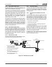
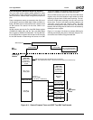
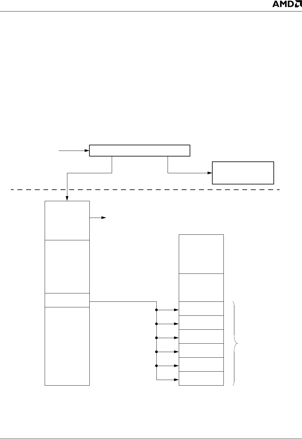
Figure 6-11 on page 173 shows an example SMI tree for
checking and clearing the source of General Purpose Tim-
ers and the User Defined Trap generated SMI.
Figure 6-11. General Purpose Timer and UDEF Trap SMI Tree Example
SMI# Asserted SMM software reads SMI Header
If Bit X = 0
(Internal SMI)
If Bit X = 1
(External SMI)
Call internal SMI handler
to take appropriate action
GX1
Core Logic
F1BAR0+I/O
Read to Clear
to determine
top-level source
of SMI
F1BAR0+I/O
Offset 06h
Read to Clear
Bits [15:10]
Bits [8:0]
Bit 9
GTMR_TRP_SMI
Offset 02h
Module
to determine
second-level
source of SMI
Bit 5
PCI_TRP_SMI
Bit 4
UDEF3_TRP_SMI
Bit 3
UDEF2_TRP_SMI
Bit 2
UDEF1_TRP_SMI
Bit 1
GPT2_SMI
Bit 0
GPT1_SMI
Take
Appropriate
Action
Other_SMI
Other_SMI
If bit 9 = 1,
Source of SMI
is GP Timer or UDEF Trap
Bits [15:6]
RSVD
Top Level Second Level
SMI De-asserted after all SMI Sources are Cleared
(i.e., Top and Second Levels - note some sources may have a Third Level)
Module


