72 AMD Geode™ SC2200 Processor Data Book
Signal Definitions
32580B
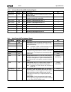
TRST# E29 I JTAG Test Reset. This signal has an internal weak pull-
up resistor.
For normal JTAG operation, this signal should be active
at power-up.
If the JTAG interface is not being used, this signal can be
tied low.
---
3.4.18 JTAG Interface Signals (Continued)
Signal Name Ball No. Type Description Mux
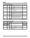
3.4.19 Test and Measurement Interface Signals
Signal Name Ball No. Type Description Mux
GXCLK V30 O GX Clock. This signal is for internal testing only. For nor-
mal operation either program as FP_VDD_ON or leave
unconnected.
FP_VDD_ON+
TEST3
TEST3 V30 O Internal Test Signals. These signals are used for inter-
nal testing only. For normal operation, leave unconnected
unless programmed as FP_VDD_ON.
FP_VDD_ON+
GXCLK
TEST2 AJ1 O Internal Test Signals. These signals are used for inter-
nal testing only. For normal operation, leave unconnected
PLL5B
TEST1 AG4 O PLL6B
TEST0 AH3 O PLL2B
GTEST F30 I Global Test. This signal is used for internal testing only.
For normal operation this signal should be pulled down
with 1.5 KΩ.
---
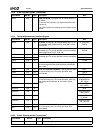
PLL6B AG4 I/O PLL6, PLL5 and PLL2 Bypass. These signals are used
for internal testing only. For normal operation leave
unconnected.
TEST1
PLL5B AJ1 I/O TEST2
PLL2B AH3 I/O TEST0
SDTEST5 D28 O Memory Internal Test Signals. These signals are used
for internal testing only. For normal operation, these sig-
nals should be programmed as one of their muxed
options.
GPIO6+
DTR2#/BOUT2+
IDE_IOR1#
SDTEST4 C31 O GPIO8+CTS2#+
IDE_DREQ1
SDTEST3 E28 O SIN2
SDTEST2 C28 O GPIO9+DCD2#+
IDE_IOW1#
SDTEST1 B29 O GPIO10+DSR2#+ID
E_IORDY1
SDTEST0 C30 O GPIO7+RTS2#+
IDE_DACK1#
TDP D30 I/O Thermal Diode Positive / Negative. These signals are
for internal testing only. For normal operation leave
unconnected.
---
TDN D31 I/O ---
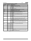
3.4.20 Power, Ground and No Connections
1
Signal Name Ball No. Type Description
AV
SSPLL2
C16 GND PLL2 Analog Ground Connection.


