


AMD Geode™ SC2200 Processor Data Book 201
Core Logic Module - Bridge, GPIO, and LPC Registers - Function 0
32580B
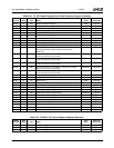
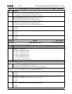
Index 40h PCI Function Control Register 1 (R/W) Reset Value: 39h
7:6 Reserved. Must be set to 0.
5 Reserved. Must be set to 0.
4 PCI Subtractive Decode.
0: Disable transfer of subtractive decode address to external PCI bus. External PCI bus is not usable.
1: Enable transfer of subtractive decode address to external PCI bus. Recommended setting.
3 Reserved. Must be set to 1.
2 Reserved. Must be set to 0.
1 PERR# Signals SERR#. Assert SERR# when PERR# is asserted or detected as active by the Core Logic module (allows
PERR# assertion to be cascaded to NMI (SMI) generation in the system).
0: Disable.
1: Enable.
0 PCI Interrupt Acknowledge Cycle Response. The Core Logic module responds to PCI interrupt acknowledge cycles.
0: Disable.
1: Enable.
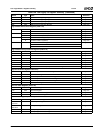
Index 41h PCI Function Control Register 2 (R/W) Reset Value: 00h
7:6 Reserved. Must be set to 0.
5 X-Bus Configuration Trap. If this bit is set to 1 and an access occurs to one of the configuration registers in PCI Function
5 (F5) register space, an SMI is generated. Writes are trapped; access to the register is denied. Reads are snooped; access
to the register is allowed.
0: Disable.
1: Enable.
Top level SMI status is reported at F1BAR0+I/O Offset 00h/02h[9].
Second level SMI status is reported at F1BAR0+I/O Offset 04h/06h[5].
4 Video Configuration Trap. If this bit is set to 1 and an access occurs to one of the configuration registers in PCI Function 4
(F4) register space, an SMI is generated.Writes are trapped; access to the register is denied. Reads are snooped; access to
the register is allowed.
0: Disable.
1: Enable.
Top level SMI status is reported at F1BAR0+I/O Offset 00h/02h[9].
Second level SMI status is reported at F1BAR0+I/O Offset 04h/06h[5].
3 Audio Configuration Trap. If this bit is set to 1 and an access occurs to one of the configuration registers in PCI Function
3 (F3) register space, an SMI is generated. Writes are trapped; access to the register is denied. Reads are snooped; access
to the register is allowed.
0: Disable.
1: Enable.
Top level SMI status is reported at F1BAR0+I/O Offset 00h/02h[9].
Second level SMI status is reported at F1BAR0+I/O Offset 04h/06h[5].
2 IDE Configuration Trap. If this bit is set to 1 and an access occurs to one of the configuration registers in PCI Function 2
(F2) register space, an SMI is generated. Writes are trapped; access to the register is denied. Reads are snooped; access
to the register is allowed.
0: Disable.
1: Enable.
Top level SMI status is reported at F1BAR0+I/O Offset 00h/02h[9].
Second level SMI status is reported at F1BAR0+I/O Offset 04h/06h[5].
1 Power Management Configuration Trap. If this bit is set to 1 and an access occurs to one of the configuration registers in
PCI Function 1 (F1) register space, an SMI is generated. Writes are trapped; access to the register is denied. Reads are
snooped; access to the register is allowed.
0: Disable.
1: Enable.
Top level SMI status is reported at F1BAR0+I/O Offset 00h/02h[9].
Second level SMI status is reported at F1BAR0+I/O Offset 04h/06h[5].
Table 6-29. F0: PCI Header/Bridge Configuration Registers for GPIO and LPC Support (Continued)
Bit Description