


80 AMD Geode™ SC2200 Processor Data Book
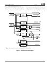
General Configuration Block
32580B
12 TRDESEL (Select TRDE#). Selects ball function.
Ball # 0: Sub-ISA Signal 1: GPIO Signal
Name Add’l Dependencies Name Add’l Dependencies
H1 / D11 TRDE# None GPIO0 None
11 EIDE (Enable IDE Outputs). This bit enables IDE output signals.
0: IDE signals are HIZ. Other signals multiplexed on the same balls are HIZ until this bit is set. (without regard to bit 24 of
this register). This bit does not control IDE channel 1 control signals selected by bit 8 of this register.
1: Signals are enabled.
10 ETFT (Enable TFT Outputs). This bit enables TFT output signals, that are multiplexed with the Parallel Port and controlled
by PMR[23].
0: Signals TFTD[17:0], TFTDE and TFTDCK are set to 0.
1: Signals TFTD[17:0], TFTDE and TFTDCK are enabled.
Note: TFTDCK that is multiplexed on IDE_RST# (ball AA1) is also enabled by this bit.
9 IOCHRDY (Select IOCHRDY). Selects ball function.
Ball # 0: PCI, GPIO Signal 1: Sub-ISA Signal
Name Add’l Dependencies Name Add’l Dependencies
H4 / C9 GPIO19 PMR[4] = 0 IOCHRDY PMR[4] = 1
INTC# PMR[4] = 1 Undefined PMR[4] = 0
8 IDE1SEL (Select IDE Channel 1). Selects IDE Channel 1 or GPIO ball functions. Works in conjunction with PMR[18] and
PMR[17], see PMR[18] and PMR[17] for definitions.
7 DOCCSSEL (Select DOCCS#). Selects DOCCS# or GPIO20 ball functions. Works in conjunction with PMR[23], see
PMR[23] for definition.
6 SP3SEL (Select UART3). Selects ball functions.
Ball # 0: IR Signals 1: Serial Port Signals
Name Add’l Dependencies Name Add’l Dependencies
J28 / AK8 IRRX1 None SIN3 None
J3 / C11 IRTX None SOUT3 None
5 IOCS0SEL (Select IOCS0#). Selects ball function. Works in conjunction with PMR[23], see PMR[23] for definition.
4 INTCSEL (Select INTC#). Selects ball function. Works in conjunction with PMR[9], see PMR[9] for definition.
3 Reserved. Write as read.
2 DOCWRSEL (Select DiskOnChip and NAND Flash Command Lines). Selects ball functions. Works in conjunction with
PMR[21], see PMR[21] for definition.
1 Reserved. Write as read.
0 PCBEEPSEL (Select PC_BEEP). Selects ball function.
Ball # 0: GPIO Signal 1: Audio Signal
Name Add’l Dependencies Name Add’l Dependencies
AL15 / V31 GPIO16 FPCI_MON = 0 PC_BEEP FPCI_MON] = 0
F_DEVSEL# FPCI_MON = 1 F_DEVSEL# FPCI_MON = 1
Offset 34h-37h Miscellaneous Configuration Register - MCR (R/W) Reset Value: 0000001h
Power-on reset value: The BOOT16 strap pin selects "Enable 16-Bit Wide Boot Memory".
31 DID0 (Ball C5) Strap Status. (Read Only) Represents the value of the strap that is latched after power-on reset. Read in
conjunction with bit 29.
30 FPCI_MON (Ball A4) Strap Status. (Read Only) Represents the value of the strap that is latched after power-on reset.
Indicates if Fast-PCI monitoring output signals (instead of Parallel Port and some audio signals) are enabled. The state of
this bit along with PMR[27] control the Fast-PCI monitoring function. See PMR[27] definition.
29 DID1 (Ball C6) Strap Status. (Read Only) Represents the value of the strap that is latched after power-on reset. Read in
conjunction with bit 31.
28:20 Reserved
19:18 Reserved. Write as 0.
17 HSYNC Timing. HSYNC timing control for TFT.
0: HSYNC timing suited for CRT.
1: HSYNC timing suited for TFT.
Table 4-2. Multiplexing, Interrupt Selection, and Base Address Registers (Continued)
Bit Description