AMD Geode™ SC2200 Processor Data Book 255
Core Logic Module - SMI Status and ACPI Registers - Function 1
32580B
6.4.2.2 ACPI Support Registers
F1 Index 40h, Base Address Register 1 (F1BAR1), points
to the base address of where the ACPI Support registers
are located. Table 6-34 shows the I/O mapped ACPI Sup-
port registers accessed through F1BAR1.
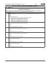
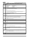
Table 6-34. F1BAR1+I/O Offset: ACPI Support Registers
Bit Description
Offset 00h-03h P_CNT — Processor Control Register (R/W) Reset Value: 00000000h
31:5 Reserved. Always reads 0.
4 THT_EN (Throttle Enable). When this bit is asserted, it enables throttling of the clock based on the CLK_VAL field (bits
[2:0] of this register).
0: Disable.
1: Enable.
If F1BAR1+I/O Offset 18h[8] =1, an SMI is generated when this bit is set.
Top level SMI status is reported at F1BAR0+I/O Offset 00h/02h[2].
Second level SMI status is reported at F1BAR0+I/O Offset 20h/22h[1].
3 Reserved. Always reads 0.
2:0 CLK_VAL (Clock Throttling Value). CPU duty cycle:
000: Reserved 010: 25% 100: 50% 110: 75%
001: 12.5% 011: 37.5% 101: 62.5% 111: 87.5%
Offset 04h Reserved Reset Value: 00h
Note: This register should not be read. It controls a reserved function of power management logic.
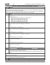
Offset 05h P_LVL3 — Enter C3 Power State Register (RO) Reset Value: xxh
7:0 P_LVL3 (Power Level 3). Reading this 8-bit read only register causes the processor to enter the C3 power state. Reads of
P_LVL3 return 0. Writes have no effect.
The ACPI state machine always waits for an SMI (any SMI) to be generated and serviced before transfer into C3 power
state.
A read of this register causes an SMI if enabled: F1BAR1+I/O Offset 18h[11] = 1 (default).
Top level SMI status is reported at F1BAR0+I/O Offset 00h/02h[2].
Second level SMI status is reported at F1BAR0+I/O Offset 20h/22h[4].
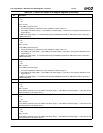
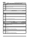
Offset 06h SMI_CMD — OS/BIOS Requests Register (R/W) Reset Value: 00h
7:0 SMI_CMD (SMI Command and OS / BIOS Requests). A write to this register stores data and a read returns the last data
written. In addition, a write to this register always generates an SMI. A read of this register does not generate an SMI.
Top level SMI status is reported at F1BAR0+I/O Offset 00h/02h[2].
Second level SMI status is reported at F1BAR0+I/O Offset 20h/22h[0].
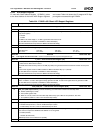
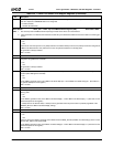
Offset 07h ACPI_FUN_CNT — ACPI Function Control Register (R/W) Reset Value: 00h
7:6 LED_CNT (LED Output Control). Controls the blinking of an LED when in the SL4 or SL5 sleep state.
00: Disable (LED# signal, is HIZ).
01: Zero (LED# signal is HIZ).
10: Blink @ 1 Hz rate, when in SL4 and SL5 sleep states. Duty cycle: LED# is 10% pulled low, 90% HIZ.
11: One (LED# is pulled low, when in SL4 and SL5 sleep states).
5 Reserved. Must be set to 0.
4 INTR_WU_SL1. Enables wakeup on enabled interrupts in sleep state SL1.
0: Disable wakeup from SL1, when an enabled interrupt is active.
1: Enable wakeup from SL1, when an enabled interrupt is active.
3 GPWIO_DBNC_DIS (GPWIO0 and GPWIO1 Debounce). When enabled, a high-to-low or low-to-high transition of greater
than 15.8 ms is required for GPWIO0 and GPWIO1 to be recognized.
0: Enable. (Default)
1: Disable. (No debounce)
GPWIO2 pin does not have debounce capability.
2:1 Reserved. Must be set to 0.


