


198 AMD Geode™ SC2200 Processor Data Book
Core Logic Module - Bridge, GPIO, and LPC Registers - Function 0
32580B
6.4 Chipset Register Space
The Chipset Register Space of the Core Logic module is
comprised of six separate functions (F0-F5), each with its
own register space. Base Address Registers (BARs) in
each PCI header register space set the base address for
the configuration registers for each respective function.
The configuration registers accessed through BARs are I/O
or memory mapped. The PCI header registers in all func-
tions are very similar.
1) Function 0 (F0): PCI Header/Bridge Configuration
Registers for GPIO, and LPC Support (see Section
6.4.1).
2) Function 1 (F1): PCI Header Registers for SMI Status
and ACPI Support (see Section 6.4.2 on page 245).
3) Function 2 (F2): PCI Header/Channel 0 and 1 Configu-
ration Registers for IDE Controller Support (see Sec-
tion 6.4.3 on page 266).
4) Function 3 (F3): PCI Header Registers for Audio Sup-
port (see Section 6.4.4 on page 272).
5) Function 4 (F4): PCI Header Registers Video Proces-
sor Support (see Section 7.3 on page 338).
6) Function 5 (F5): PCI Header Registers for X-Bus
Expansion Support (see Section 6.4.5 on page 287).
Function 5 contain six BARs in their standard PCI
header locations (i.e., Index 10h, 14h, 18h, 1Ch, 20h,
and 24h). In addition there are six mask registers that
allow the six BARs to be fully programmable from 4
GB to 16 bytes for memory and from 4 GB to 4 bytes
for I/O
General Remarks:
• Reserved bits that are defined as “must be set to 0 or 1"
should be written with that value.
• Reserved bits that are not defined as “must be set to 0
or 1" should be written with a value that is read from
them.
• “Read to Clear” registers that are wider than one byte
should be read in one read operation. If they are read a
byte at a time, status bits may be lost, or not cleared.
6.4.1 Bridge, GPIO, and LPC Registers -
Function 0
The register space designated as Function 0 (F0) is used
to configure Bridge features and functionality unique to the
Core Logic module. In addition, it configures the PCI por-
tion of support hardware for the GPIO and LPC support
registers. The bit formats for the PCI Header and Bridge
Configuration registers are given in Table 6-29.
Note: The registers at F0 Index 50h-FFh can also be
accessed at F1BAR0+I/O Offset 50h-FFh. How-
ever, the preferred method is to program these
registers through the F0 register space.
Located in the PCI Header registers of F0, are two Base
Address Registers (F0BARx) used for pointing to the regis-
ter spaces designated for GPIO and LPC configuration
(described in Section 6.4.1.1 "GPIO Support Registers" on
page 233 and Section 6.4.1.2 "LPC Support Registers" on
page 237).
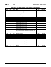
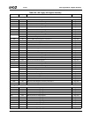
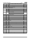
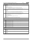
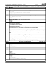
Table 6-29. F0: PCI Header/Bridge Configuration Registers for GPIO and LPC Support
Bit Description
Index 00h-01h Vendor Identification Register (RO) Reset Value: 100Bh
Index 02h-03h Device Identification Register (RO) Reset Value: 0500h
Index 04h-05h PCI Command Register (R/W) Reset Value: 000Fh
15:10 Reserved. Must be set to 0.
9 Fast Back-to-Back Enable. This function is not supported when the Core Logic module is a master. It must always be dis-
abled (i.e., must be set to 0).
8 SERR#. Allow SERR# assertion on detection of special errors.
0: Disable. (Default)
1: Enable.
7 Wait Cycle Control. (Read Only) This function is not supported in the Core Logic module. It is always disabled (always
reads 0, hardwired).
6 Parity Error. Allow the Core Logic module to check for parity errors on PCI cycles for which it is a target and to assert
PERR# when a parity error is detected.
0: Disable. (Default)
1: Enable.
5 VGA Palette Snoop Enable. (Read Only) This function is not supported in the Core Logic module. It is always disabled
(always reads 0, hardwired).