AMD Geode™ SC2200 Processor Data Book 153
Core Logic Module
32580B
value is listed because both data and command timings are
the same mode. However, the actual timing value for the
Mode 4 device would be constructed out of the Mode 4
data timing 16-bit value and the Mode 0 16-bit command
timing value. Both 16-bit values are shown in the register
description but not assembled together as they are mixed
modes.
6.2.3.3 Bus Master Mode
Two IDE bus masters are provided to perform the data
transfers for the primary and secondary channels. The IDE
controller of the Core Logic module off-loads the CPU and
improves system performance in multitasking environ-
ments.
The bus master mode programming interface is an exten-
sion of the standard IDE programming model. This means
that devices can always be dealt with using the standard
IDE programming model, with the master mode functional-
ity used when the appropriate driver and devices are
present. Master operation is designed to work with any IDE
device that supports DMA transfers on the IDE bus.
Devices that work in PIO mode can only use the standard
IDE programming model.
The IDE bus masters use a simple scatter/gather mecha-
nism allowing large transfer blocks to be scattered to or
gathered from memory. This cuts down on the number of
interrupts to and interactions with the CPU.
Physical Region Descriptor Table Address
Before the controller starts a master transfer it is given a
pointer to a Physical Region Descriptor Table. This pointer
sets the starting memory location of the Physical Region
Descriptors (PRDs). The PRDs describe the areas of mem-
ory that are used in the data transfer. The PRDs must be
aligned on a 4-byte boundary and the table cannot cross a
64 KB boundary in memory.
Primary and Secondary IDE Bus Master Registers
The IDE Bus Master Registers for each channel (primary
and secondary) have an IDE Bus Master Command regis-
ter and Bus Master Status register. These registers and bit
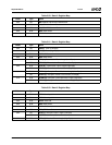
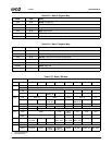
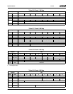
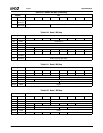
formats are described in Table 6-36 on page 270.
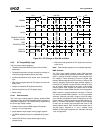
Physical Region Descriptor Format
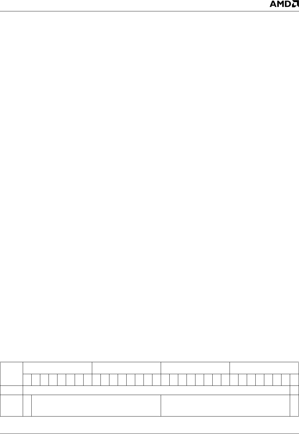
Each physical memory region to be transferred is
described by a Physical Region Descriptor (PRD) as illus-
trated in Table 6-1. When the bus master is enabled (Com-
mand register bit 0 = 1), data transfer proceeds until each
PRD in the PRD table has been transferred. The bus mas-
ter does not cache PRDs.
The PRD table consists of two DWORDs. The first DWORD
contains a 32-bit pointer to a buffer to be transferred. The
second DWORD contains the size (16 bits) of the buffer
and the EOT flag. The EOT bit (bit 31) must be set to indi-
cate the last PRD in the PRD table.
Programming Model
The following steps explain how to initiate and maintain a
bus master transfer between memory and an IDE device.
1) Software creates a PRD table in system memory.
Each PRD entry is 8 bytes long, consisting of a base
address pointer and buffer size. The maximum data
that can be transferred from a PRD entry is 64 KB. A
PRD table must be aligned on a 4-byte boundary. The
last PRD in a PRD table must have the EOT bit set.
2) Software loads the starting address of the PRD table
by programming the PRD Table Address register.
3) Software must fill the buffers pointed to by the PRDs
with IDE data.
4) Write 1 to the Bus Master Interrupt bit and Bus Master
Error (Status register bits 2 and 1) to clear the bits.
5) Set the correct direction to the Read or Write Control
bit (Command register bit 3).
Engage the bus master by writing a “1” to the Bus
Master Control bit (Command register bit 0).
The bus master reads the PRD entry pointed to by the
PRD Table Address register and increments the
address by 08h to point to the next PRD. The transfer
begins.
6) The bus master transfers data to/from memory
responding to bus master requests from the IDE
device. At the completion of each PRD, the bus mas-
ter’s next response depends on the settings of the
EOT flag in the PRD. If the EOT bit is set, then the IDE
bus master clears the Bus Master Active bit (Status
register bit 0) and stop. If any errors occurred during
the transfer, the bus master sets the Bus Master Error
bit Status register bit 1).
Table 6-1. Physical Region Descriptor Format
DWORD
Byte 3 Byte 2 Byte 1 Byte 0
31 31 29 28 27 26 25 24 23 22 21 20 19 18 17 16 15 14 13 12 11 10 9 8 7 6 5 4 3 2 1 0
0 Memory Region Physical Base Address [31:1] (IDE Data Buffer) 0
1E
O
T
Reserved Size [15:1] 0


