


292 AMD Geode™ SC2200 Processor Data Book
Core Logic Module - USB Controller Registers - PCIUSB
32580B
6.4.6 USB Controller Registers - PCIUSB
The registers designated as PCIUSB are 32-bit registers
decoded from the PCI address bits [7:2] and C/BE[3:0]#,
when IDSEL is high, AD[10:8] select the appropriate func-
tion, and AD[1:0] are 00.
The PCI Configuration registers are listed in Table 6-41.
They can be accessed as any number of bytes within a sin-
gle 32-bit aligned unit. They are selected by the PCI-stan-
dard Index and Byte-Enable method.
In the PCI Configuration space, there is one Base Address
Register (BAR), at Index 10h, which is used to map the
USB Host Controller's operational register set into a 4K
memory space. Once the BAR register has been initialized,
and the PCI Command register at Index 04h has been set
to enable the Memory space decoder, these “USB Control-
ler” registers are accessible.
The memory-mapped USB Controller registers are listed in
Table 6-42. They follow the Open Host Controller Interface
(OHCI) specification. Registers marked as “Reserved”, and
reserved bits within a register, should not be changed by
software.
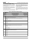
Table 6-41. PCIUSB: USB PCI Configuration Registers
Bit Description
Index 00h-01h Vendor Identification Register (RO) Reset Value: 0E11h
Index 02h-03h Device Identification Register (RO) Reset Value: A0F8h
Index 04h-05h Command Register (R/W) Reset Value: 00h
15:10 Reserved. Must be set to 0.
9 Fast Back-to-Back Enable. (Read Only) USB only acts as a master to a single device, so this functionality is not needed.
It is always disabled (i.e., this bit must always be set to 0).
8 SERR#. When this bit is enabled, USB asserts SERR# when it detects an address parity error.
0: Disable.
1: Enable.
7 Wait Cycle Control. USB does not need to insert a wait state between the address and data on the AD lines. It is always
disabled (i.e., this bit is set to 0).
6 Parity Error. USB asserts PERR# when it is the agent receiving data and it detects a data parity error.
0: Disable.
1: Enable.
5 VGA Palette Snoop Enable. (Read Only) USB does not support this function. It is always disabled (i.e., this bit is set to
0).
4 Memory Write and Invalidate. Allow USB to run Memory Write and Invalidate commands.
0: Disable.
1: Enable.
The Memory Write and Invalidate Command only occurs if the cache-line size is set to 32 bytes and the memory write is
exactly one cache line.
This bit must be set to 0.
3 Special Cycles. USB does not run special cycles on PCI. It is always disabled (i.e., this bit is set to 0).
2 PCI Master Enable. Allow the USB to run PCI master cycles.
0: Disable.
1: Enable.
1 Memory Space. Allow the USB to respond as a target to memory cycles from the PCI bus.
0: Disable.
1: Enable.
0 I/O Space. Allow the USB to respond as a target to I/O cycles from the PCI bus.
0Disable.
1: Enable.