


AMD Geode™ SC2200 Processor Data Book 407
Electrical Specifications
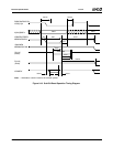
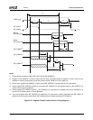
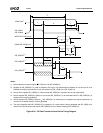
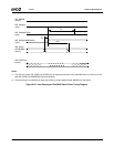
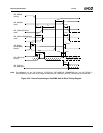
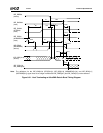
32580B
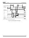
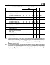
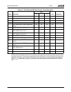
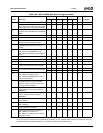
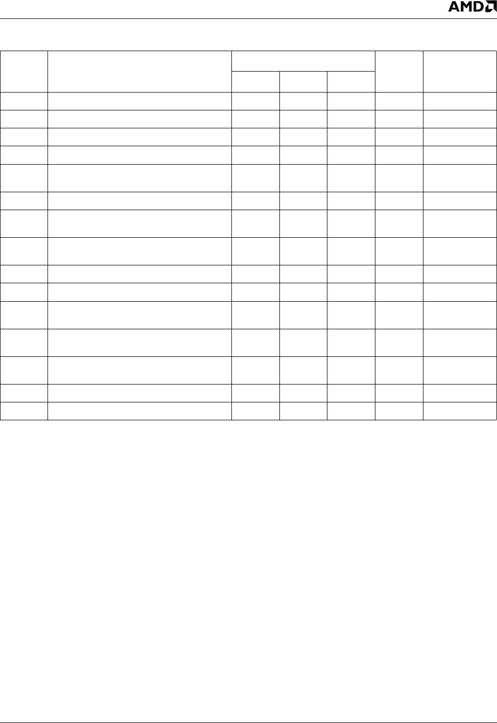
Table 9-27. IDE Multiword DMA Data Transfer Timing Parameters
Symbol Parameter
Mode
Unit Comments012
t
0
Cycle time (min) 480 150 120 ns Note 1
t
D
IDE_IOR[0:1]#/IDE_IOW[0:1]# (min) 215 80 70 ns
t
E
IDE_IOR[0:1]# data access (max) 150 60 50 ns
t
F
IDE_IOR[0:1]# data hold (min) 5 5 5 ns
t
G
IDE_IOW[0:1]#/IDE_IOW[0:1]# data setup
(min)
100 30 20 ns
t
H
IDE_IOW[0:1]# data hold (min) 20 15 10 ns
t
I
IDE_DACK[0:1]# to IDE_IOR[0:1]#/
IDE_IOW[0:1]# setup (min)
000ns
t
J
IDE_IOR[0:1]#/IDE_IOW[0:1]# to
IDE_DACK[0:1]# hold (min)
20 5 5 ns
t
KR
IDE_IOR[0:1]# negated pulse width (min) 50 50 25 ns
t
KW
IDE_IOW[0:1]# negated pulse width (min) 215 50 25 ns
t
LR
IDE_IOR[0:1]# to IDE_DREQ[0:1] delay
(max)
120 40 35 ns
t
LW
IDE_IOW[0:1]# to IDE_DREQ0,1 delay
(max)
40 40 35 ns
t
M
IDE_CS[0:1]# valid to IDE_IOR[0:1]#/
IDE_IOW[0:1]# (min)
50 30 25 ns
t
N
IDE_CS[0:1]# hold 15 10 10 ns
t
Z
IDE_DACK[0:1]# to TRI-STATE 20 25 25 ns
Note 1. t
0
is the minimum total cycle time, t
D
is the minimum command active time, and t
KR
or t
KW
is the minimum command
recovery time or command inactive time. The actual cycle time equals the sum of the command active time and the
command inactive time. The three timing requirements of t
0
, t
D
and t
KR/KW
, are met. The minimum total cycle time
requirement t
0
is greater than the sum of t
D
and t
KR/KW
. (This means that a host implementation can lengthen t
D
and/or t
KR/KW
to ensure that t
0
is equal to or greater than the value reported in the device’s IDENTIFY DEVICE
data.)