100 AMD Geode™ SC2200 Processor Data Book
SuperI/O Module
32580B
5.4 Standard Configuration Registers
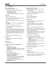
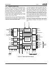
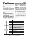
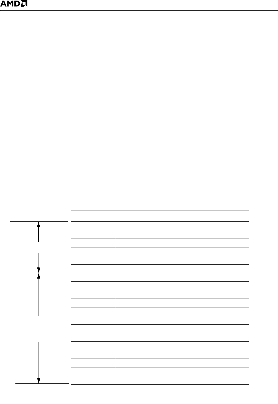
As illustrated in Figure 5-4, the Standard Configuration reg-
isters are broadly divided into two categories: SIO Control
and Configuration registers and Logical Device Control and
Configuration registers (one per logical device, some are
optional).
SIO Control and Configuration Registers
The only PnP control register in the SIO module is the Log-
ical Device Number register at Index 07h. All other stan-
dard PnP control registers are associated with PnP
protocol for ISA add-in cards, and are not supported by the
SIO module.
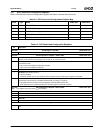
The SIO Configuration registers at Index 20h-27h are
mainly used for part identification. (See Section 5.4.1 "SIO
Control and Configuration Registers" on page 103 for fur-
ther details.)
Logical Device Control and Configuration Registers
A subset of these registers is implemented for each logical
device. (See Table 5-2 on page 98 for LDN assignment and
Section 5.4.2 "Logical Device Control and Configuration"
on page 104 for register details.)
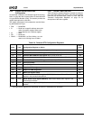
Logical Device Control Register (Index 30h): The only
implemented Logical Device Control register is the Activate
register at Index 30. Bit 0 of the Activate register and bit 0
of the SIO Configuration 1 register (Global Device Enable
bit) control the activation of the associated function block
(except for the RTC and the SWC). Activation of the block
enables access to the block’s registers, and attaches its
system resources, which are unused as long as the block is
not activated. Activation of the block may also result in
other effects (e.g., clock enable and active signaling), for
certain functions.
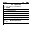
Standard Logical Device Configuration Registers
(Index 60h-75h): These registers are used to manage the
resource allocation to the functional blocks. The I/O port
base address descriptor 0 is a pair of registers at Index
60h-61h, holding the (first or only) 16-bit base address for
the register set of the functional block. An optional second
base-address (descriptor 1) at Index 62h-63h is used for
devices with more than one continuous register set. Inter-
rupt Number Select (Index 70h) and Interrupt Type Select
(Index 71h) allocate an IRQ line to the block and control its
type. DMA Channel Select 0 (Index 74h) allocates a DMA
channel to the block, where applicable. DMA Channel
Select 1 (Index 75h) allocates a second DMA channel,
where applicable.
Special Logical Device Configuration Registers (F0h-
F3h): The vendor-defined registers, starting at Index F0h
are used to control function-specific parameters such as
operation modes, power saving modes, pin TRI-STATE,
clock rate selection, and non-standard extensions to
generic functions.
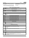
Figure 5-4. Standard Configuration Registers Map
SIO Control and
Configuration Registers
Logical Device Control and
one per logical device
Configuration Registers -
Index Register Name
07h Logical Device Number
20h SIO ID
21h SIO Configuration 1
22h SIO Configuration 2
27h SIO Revision ID
2Eh Reserved exclusively for AMD use
30h Logical Device Control (Activate)
60h I/O Port Base Address Descriptor 0 Bits [15:8]
61h I/O Port Base Address Descriptor 0 Bits [7:0]
62h I/O Port Base Address Descriptor 1 Bits [15:8]
63h I/O Port Base Address Descriptor 1 Bits [7:0]
70h Interrupt Number Select
71h Interrupt Type Select
74h DMA Channel Select 0
75h DMA Channel Select 1
F0h Device Specific Logical Device Configuration 1
F1h Device Specific Logical Device Configuration 2
F2h Device Specific Logical Device Configuration 3
F3h Device Specific Logical Device Configuration 4
(some are optional)


